6 crucial steps in semiconductor manufacturing
Deposition, resist, lithography, etch, ionization, packaging: the steps in microchip production you need to know about
Updated - 10:00, October 4, 2023
By now you’ll have heard word on the street: a new iPhone 15 is here. But it’s under the hood of this iPhone – and other digital devices – where things really get interesting. That’s where top-of-the-line chips like Apple’s A17 Pro and A16 Bionic SoCs are making new, innovative technology possible. So how are these chips made and what are the most important steps?
We don’t need to tell you that modern digital devices – smartphones, PCs, gaming consoles and more – are powerful pieces of technology. Much of this power comes from microchips, some of the smallest but most detailed pieces of tech that exist. In 2021, semiconductor unit sales reached a record 1.15 trillion shipments. That’s about 145 chips for every person on earth. But despite what their widespread presence might suggest, manufacturing a microchip is no mean feat. To make any chip, numerous processes play a role. Let’s discuss six critical semiconductor manufacturing steps: deposition, photoresist, lithography, etch, ionization and packaging.
Illustration by Aad Goudappel
Deposition
The process begins with a silicon wafer. Wafers are sliced from a salami-shaped bar of 99.99% pure silicon (known as an 'ingot') and polished to extreme smoothness. Thin films of conducting, isolating or semiconducting materials – depending on the type of structure being made – are deposited on the wafer to enable the first layer to be printed on it. This important step is commonly known as 'deposition'.
As microchip structures 'shrink', the process of patterning the wafer becomes more complex. Advances in deposition, as well as etch and lithography – more on that later – are enablers of shrink and the pursuit of Moore's Law. These advances include the use of new materials and innovations that enable increased precision when depositing these materials.
Photoresist coating
The wafer is then covered with a light-sensitive coating called 'photoresist', or 'resist' for short. There are two types of resist: positive and negative.
The main difference between positive and negative resist is the chemical structure of the material and the way that the resist reacts with light. With positive resist, the areas exposed to ultraviolet light change their structure and are made more soluble – ready for etching and deposition. The opposite is true for negative resist, where areas hit by light polymerize, meaning they become stronger and more difficult to dissolve. Positive resist is most commonly used in semiconductor manufacturing because its higher resolution capability makes it the better choice for the lithography stage.
Several companies around the world produce resist for semiconductor manufacturing, such as Fujifilm Electronics Materials, The Dow Chemical Company and JSR Corporation.
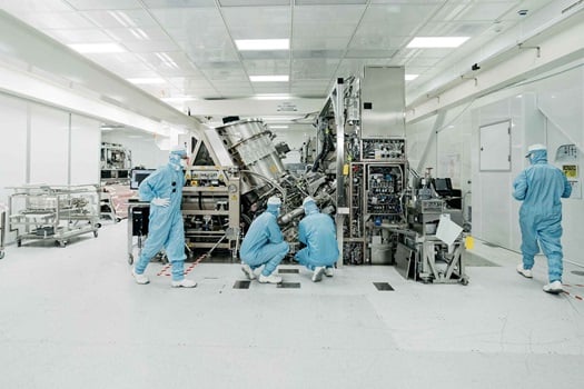
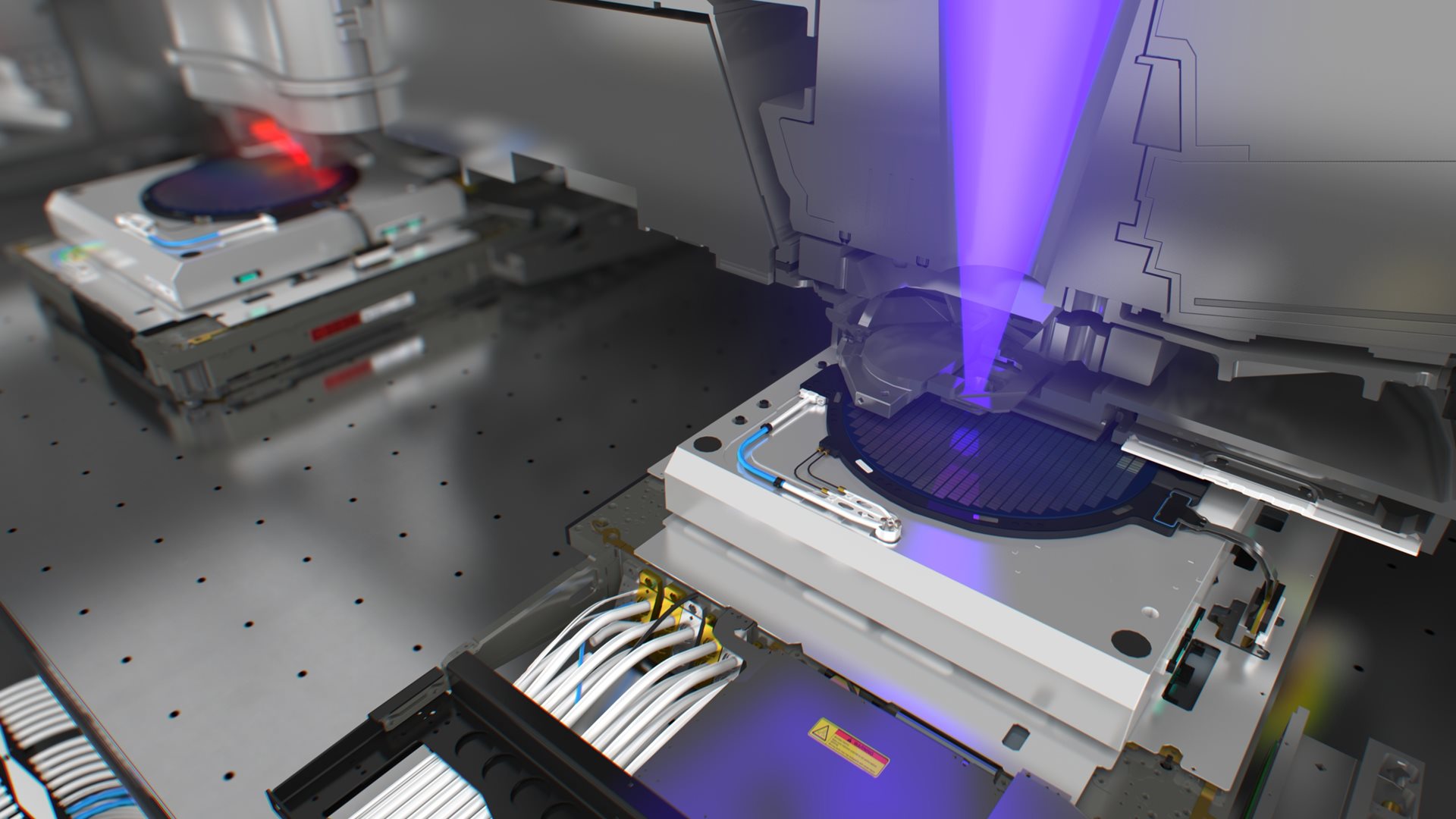
Lithography
Lithography is a crucial step in the chipmaking process, because it determines just how small the transistors on a chip can be. During this stage, the chip wafer is inserted into a lithography machine (that's us!) where it's exposed to deep ultraviolet (DUV) or extreme ultraviolet (EUV) light. This light has a wavelength anywhere from 365 nm for less complex chip designs to 13.5 nm, which is used to produce some of the finest details of a chip – some of which are thousands of times smaller than a grain of sand.
Light is projected onto the wafer through the 'reticle', which holds the blueprint of the pattern to be printed. The system's optics (lenses in a DUV system and mirrors in an EUV system) shrink and focus the pattern onto the resist layer. As explained earlier, when light hits the resist, it causes a chemical change that enables the pattern from the reticle to be replicated onto the resist layer.
Getting the pattern exactly right every time is a tricky task. Particle interference, refraction and other physical or chemical defects can occur during this process. That's why, sometimes, the pattern needs to be optimized by intentionally deforming the blueprint, so you're left with the exact pattern that you need. Our systems do this by combining algorithmic models with data from our systems and test wafers in a process referred to as 'computational lithography'. The resulting blueprint might look different from the pattern it eventually prints, but that's exactly the point. Everything we do is focused on getting the printed patterns just right.
Etch
The next step is to remove the degraded resist to reveal the intended pattern. During 'etch', the wafer is baked and developed, and some of the resist is washed away to reveal a 3D pattern of open channels. Etch processes must precisely and consistently form increasingly conductive features without impacting the overall integrity and stability of the chip structure. Advanced etch technology is enabling chipmakers to use double, quadruple and spacer-based patterning to create the tiny features of the most modern chip designs.
As with resist, there are two types of etch: 'wet' and 'dry'. Dry etching uses gases to define the exposed pattern on the wafer. Wet etching uses chemical baths to wash the wafer. Companies such as Lam Research, Oxford Instruments and SEMES develop semiconductor etching systems.

Chips are made up of dozens of layers. So, it's important that etching is carefully controlled so as not to damage the underlying layers of a multilayer microchip structure or – if the etching is intended to create a cavity in the structure – to ensure the depth of the cavity is exactly right. When you consider that some microchip designs such as 3D NAND are reaching up to 175 layers, this step is becoming increasingly important – and difficult.
Ion implantation
Once patterns are etched in the wafer, the wafer may be bombarded with positive or negative ions to tune the electrical conducting properties of part of the pattern. Raw silicon – the material the wafer is made of – is not a perfect insulator or a perfect conductor. Silicon’s electrical properties are somewhere in between. Directing electrically charged ions into the silicon crystal allows the flow of electricity to be controlled and transistors – the electronic switches that are the basic building blocks of microchips – to be created. This process is known as ‘ion implantation’.
After the ions are implanted in the layer, the remaining sections of resist that were protecting areas that should not be modified are removed.
Packaging
The entire process of creating a silicon wafer with working chips consists of thousands of steps and can take more than three months from design to production. To get the chips out of the wafer, it is sliced and diced with a diamond saw into individual chips. Cut from a 300-mm wafer, the size most often used in semiconductor manufacturing, these so-called 'dies' differ in size for various chips. Some wafers can contain thousands of chips, while others contain just a few dozen.
The chip die is then placed onto a 'substrate'. This is a type of baseboard for the microchip die that uses metal foils to direct the input and output signals of a chip to other parts of a system. And to close the lid, a 'heat spreader' is placed on top. This heat spreader is a small, flat metal protective container holding a cooling solution that ensures the microchip stays cool during operation.
Wiliot, Ayar Labs, SPTS Technologies, Applied Materials: these are just some of the names in the microchip packaging business, but there are many more.
Just the beginning
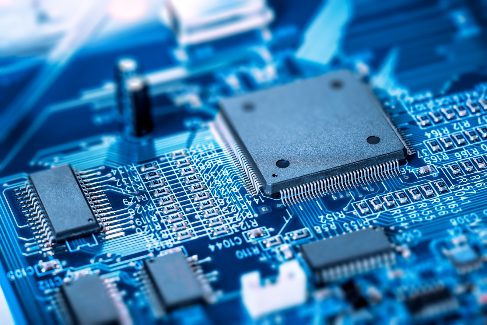
The microchip is now ready to get to work as part of your smartphone, TV, tablet or any other electronic device. It’s probably only about the size of your thumb, but one chip can contain billions of transistors. For example, Apple’s A16 Bionic system-on-a-chip contains 16 billion transistors and can perform 17 trillion operations per second.
Of course, semiconductor manufacturing involves far more than just these steps. There's also measurement and inspection, electroplating, testing and much more. And each microchip goes through this process hundreds of times before it becomes part of a device.
Are you ready to dive a little deeper into the world of chipmaking? Discover how chips are made.
Be the first to know about new stories!
About the author

- Alison Li
- Writer & editor
- Alison is passionate about creative writing, content marketing and social media. Outside of work, she enjoys watching anime and playing video games.

- Jessica Timings
- Editor & writer
- Born in Aotearoa New Zealand and based in the Netherlands, Jessica is a humanitarian who has launched into the tech industry. A curious storyteller at heart, she is fascinated by ASML’s mind-blowing technology and the people behind these innovations.