6-minute read - by Sander Hofman, May 7, 2021
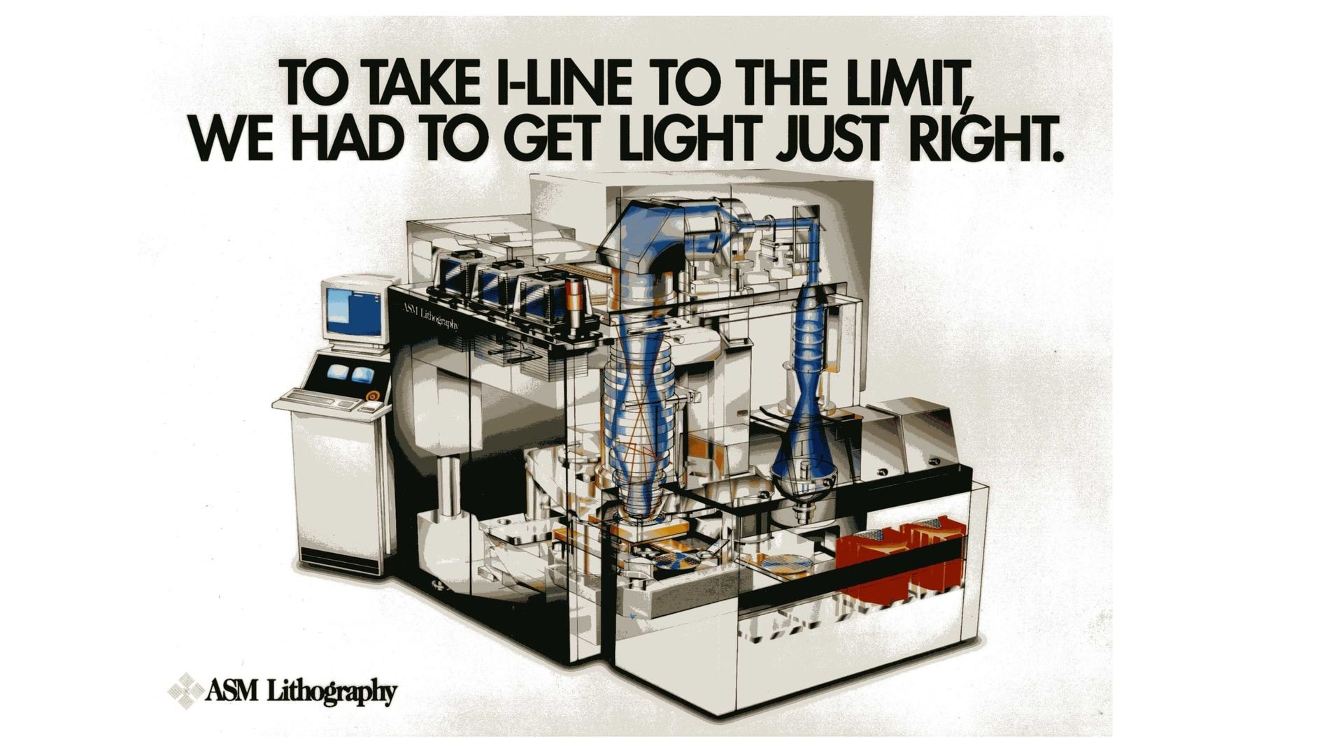
May 9, 2021 marks 30 years since the first-ever PAS 5500 platform was shipped. PAS 5500 shaped ASML’s market success and technology leadership – becoming our longest-lived lithography platform and one of our most versatile product lines.
The PAS 5500 is the platform that made ASML’s name. Before its launch, ASML was a distant third in the lithography market, behind the giants Nikon and Canon. But the success of the PAS 5500 platform soon moved ASML up to second and laid the foundation for its growth to become the global leader in lithography.
After three decades, it would be fair to say that each PAS system has its own unique story to tell, as it moved through decades of semiconductor manufacturing. Like the 25-year-old PAS 5500/275 system that, after many years in memory and radio frequency (RF) module production, was recently refurbished and resold to start a new life at the forefront of the virtual reality boom.
The story of this system and many others proves how relevant PAS 5500 continues to be for the semiconductor industry. TWINSCAN is now the platform of choice for high-volume semiconductor manufacturing and at the leading edge of Moore’s Law. And although the PAS 5500 is no longer made as new, its low cost, small size, simplicity and robustness mean that a refurbished PAS 5500 is often the preferred option in various niche applications. In fact, it’s still so relevant to chip manufacturing that ASML has extended the customer service of its oldest product line to 2030 and beyond.
Success from the start
The PAS 5500 comes from a long line of systems initiated by researchers at Philips in the 1970s. The name of the platform itself speaks to its legacy and our long relationship with Philips: the Philips Automatic Stepper (PAS).
Longtime employee and current manager of Mature Product Sales at ASML, Ted Shafer has been closely involved with this breakthrough platform for his whole career.
“I joined ASML the same year the PAS 5500 was launched – 1991,” Ted recalls. “My first job was as an application engineer, accompanying the first-ever PAS 5500 shipment which went to IBM in Fishkill in the United States. My role was to optimize system performance and help bring the novel system to production-level maturity in the customer’s fab.”
Those first PAS 5500 systems, and Ted’s efforts in optimizing them, led to IBM introducing its System/390 family, which at that time were, in their words, “the most powerful computers IBM has ever offered”.
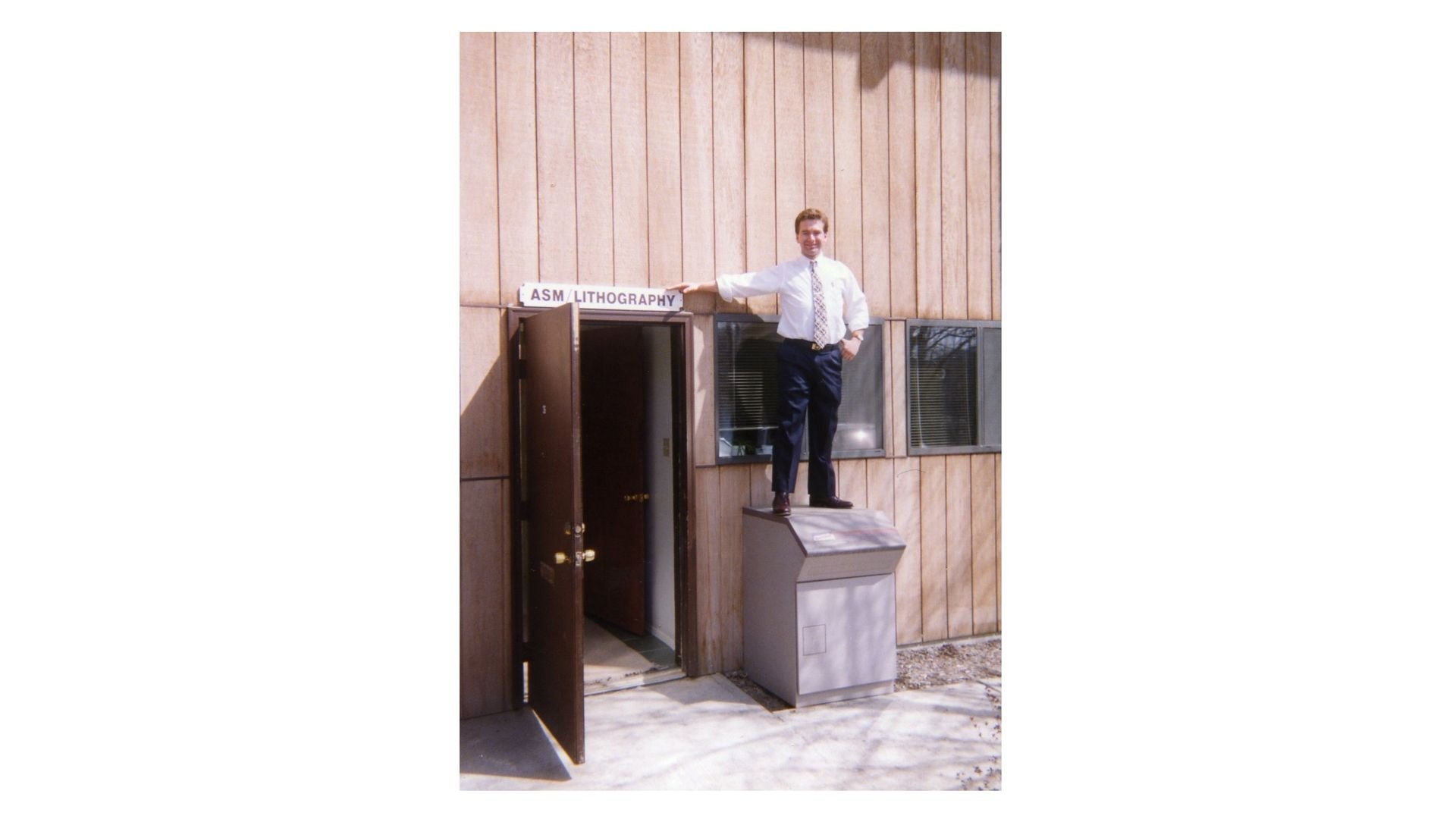
installed.
As the PAS 5500 evolved so did Ted’s career with ASML, but the platform was never far away. By 1996, Ted had moved into sales where, among many other things, he was involved in selling some of the first PAS 5500/200 systems with an ‘i-line’ light source to Micron. It was one of these systems that 25 years later, after refurbishment and upgrade, would begin its third life helping to realize virtual reality technology.
Life at the cutting edge
Micron is one of the world’s largest producers of computer memory and storage. It was also ASML’s largest customer at that time and therefore instrumental in the PAS 5500 platform’s success.
“Micron got early access to the latest technology and, in return, we got valuable feedback that would help us improve the performance of our systems,” Ted explains. “They invested so heavily in the PAS 5500/200 that they had to update their accounting software to accommodate deals above a certain value.”
Initially, Micron used the PAS 5500/200, which had a resolution of 0.35 µm, to create the critical layers in its cutting-edge memory chips of the day. And as time, technology and market demands moved on, ASML’s PAS 5500 supported these developments through continuous improvement – in this case, introducing higher resolution i-line systems as well as krypton fluoride (KrF) and argon fluoride (ArF) systems to support even finer resolutions.
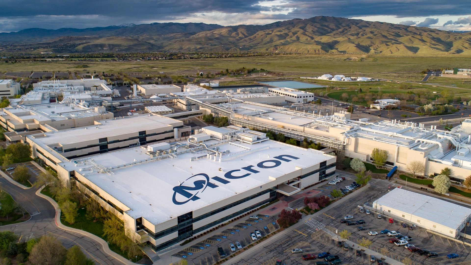
factory.
Value beyond critical
As new systems come online in fabs to produce the critical layers of more advanced chips, older systems remain in constant use but migrate to the lithography of choice for less critical layers. This was the case for Micron’s PAS 5500/200 systems.
However, in 2000, there was a major industry switch from 200 mm wafers to 300 mm wafers to support higher chip outputs and improve cost efficiency. Many of ASML’s larger customers, decided to migrate their production to the TWINSCAN platform which, unlike the PAS 5500, supported the larger wafers. Over the next few years, Micron sold off its 200 mm wafer processing equipment base.
“By 2011, I had moved from ASML to an investment bank that offered financial services such as leasing and remarketing to semiconductor companies. Micron was one of our remarketing clients, and I was responsible for selling one of their PAS 5500/200 systems to another customer,” Ted adds.
This is an example of the ‘equipment cascade’ that is quite common in the semiconductor industry, and which enables manufacturers of all sizes and market types to maximize the value of their equipment. Typically, a leading-edge customer may get 10 to 15 years of service from a new lithography system at different layers of criticality. Then they sell it on to manufacturers who aren’t trying to push Moore’s Law, but are active in the so-called ‘More than Moore’ market. This is a field where digital electronics meet the analog world, like sensor chips for automotive, micro electromechanical (MEMS) chips such as accelerometers, ultra-low-power chips, and chips for RF identification.
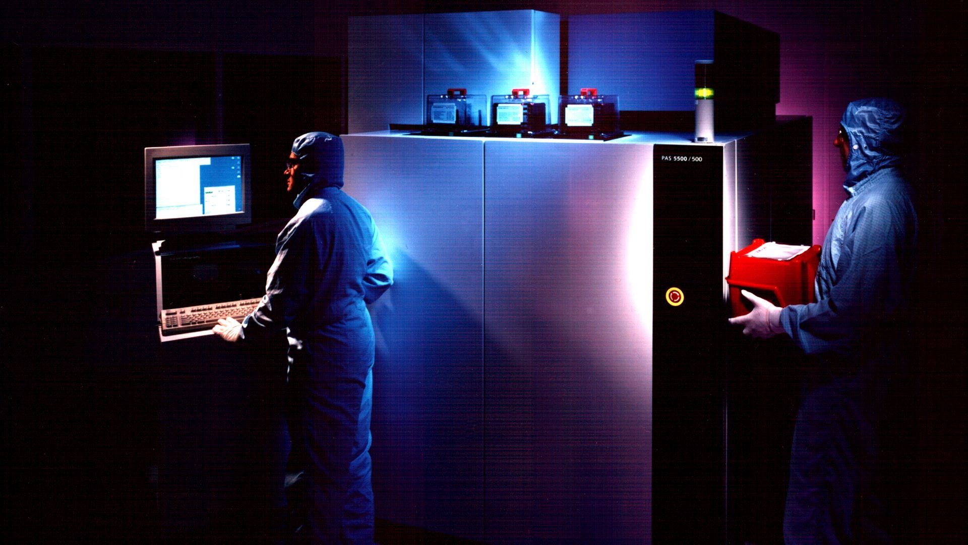
Chipmakers of these specialty semiconductors still care about size, speed and power, but they do not necessarily need the cutting-edge lithography that creates the finest geometries at the most advanced nodes. PAS 5500 is the ideal platform for these chipmakers – offering both affordability and the required productivity.
Resell, refurbish, recycle
As an alternative to direct reselling, some chip manufacturers choose to sell their surplus lithography systems back to ASML.
ASML has long been active in the used lithography equipment market. It has refurbished and resold well over 500 PAS 5500 systems. Unlike direct reselling, when ASML refurbishes a system it can guarantee the original specifications and provide a full warranty. This gives the buyer confidence that they are getting a reliable, high-quality system.
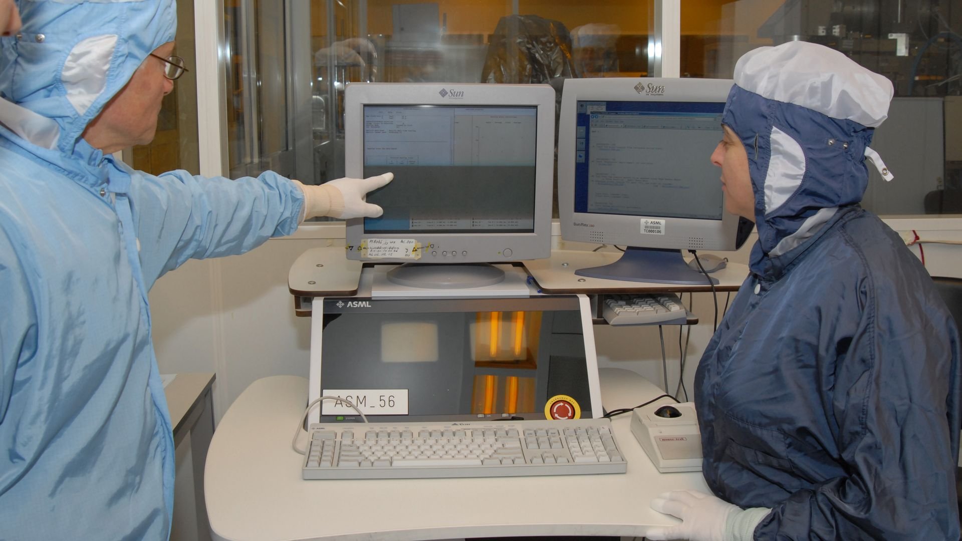
“More than 90% of the PAS 5500s we have ever built are still in use, whether as refurbished tools or as the recycled heart of a new system.”
Depending on market requirements at the time, when refurbishing a machine ASML may also reconfigure it to higher specifications, upgrade it to a newer model type or even convert it to a new wavelength. Since 2009, all new PAS 5500 systems supplied to the market have been built by buying cores from the installed base and recycling them.
“More than 90% of the PAS 5500s we have ever built are still in use, whether as refurbished tools or as the recycled heart of a new system. As well as ensuring value for buyers and sellers, this approach has a positive impact on the ‘green economy’ of the semiconductor industry by minimizing both demand for new materials and the amount of waste which needs to be disposed,” Ted explains.
A new life
And so, the system that started at Micron and then had a second life at another customer was refurbished and upgraded to a PAS 5500/275 – a model for which Ted helped to write the original specifications. It is still an i-line stepper, but now offers resolutions down to 0.28 µm and throughput of up to 100 wafers per hour.
Having returned to ASML, Ted once again oversaw the sale of the system to another major technology company where it has started a third life, helping the company produce innovative chips for virtual reality applications.
What’s so special about this one system that makes it so long-lived? In truth, nothing. The story of its life is par for the course for PAS 5500 systems – many have similar stories. Which is why, as this remarkable platform turns 30, it is still going strong and helping to meet growing demand for sensors, MEMS, chips, photonics and more.
