Specialty applications are devices designed for specific functions beyond mainstream logic and memory manufacturing.
They demand capabilities that go beyond standard lithography because they often use non-standard materials such as Silicon Carbide (SiC), Galium Nitride (GaN), Indium Phosphide (InP) or piezoelectric substrates, and require support for thick, thin and bowed wafers with specific imaging, alignment and overlay capabilities.
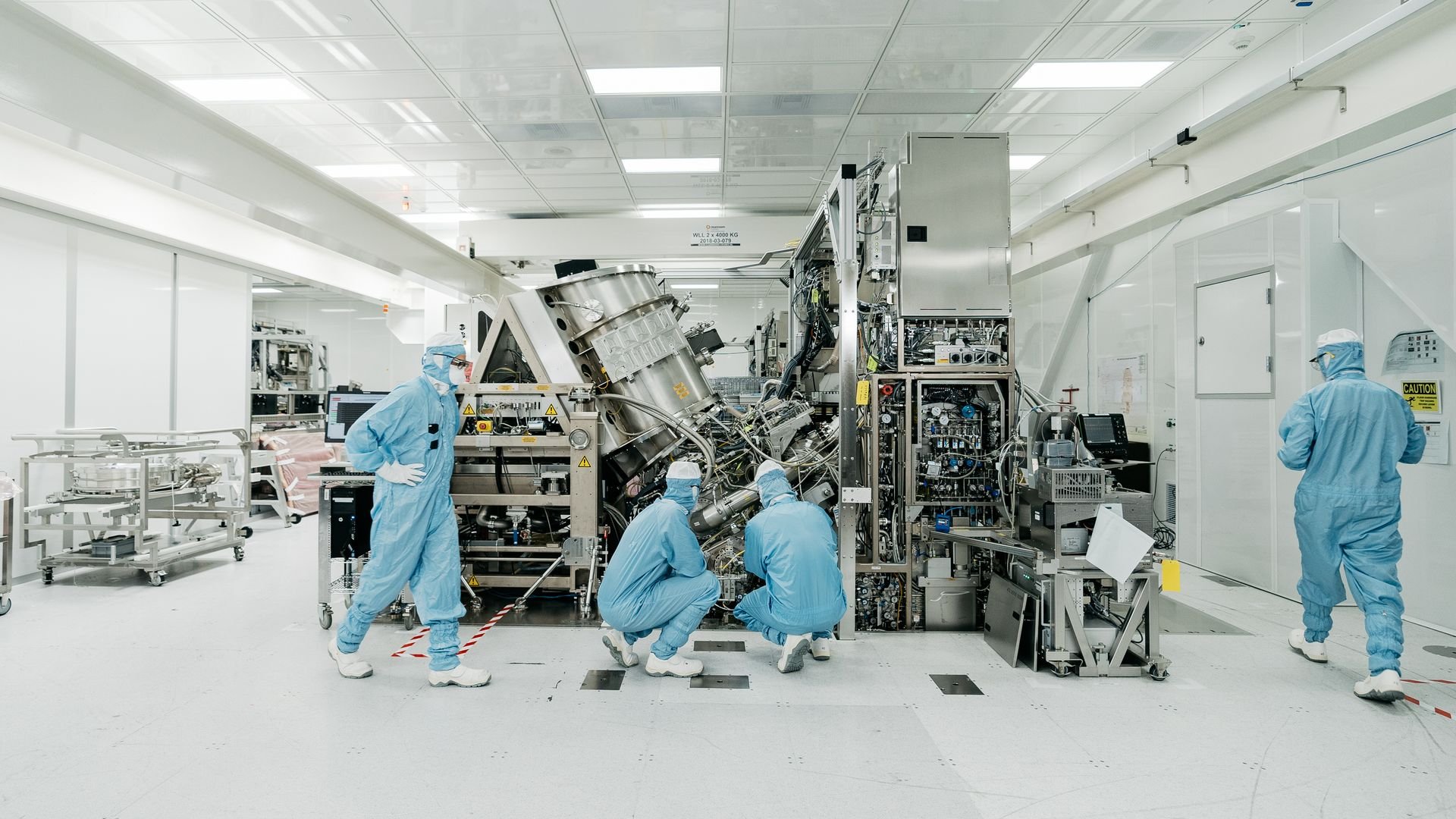
The PAS 5500 is a proven ASML DUV platform optimized for these diverse manufacturing requirements and widely deployed in mature-node semiconductor manufacturing.
Supporting process technologies down to 90nm, it enables cost-effective production of many More-than-Moore applications such as photonics, analog, power, TFH, RF Filters, MEMS, and MicroLED on wafer sizes up to 200 mm.
Built for flexibility. Ready for what’s next
Since its introduction in 1991, the PAS 5500 platform has remained a trusted choice for manufacturers pushing the boundaries of innovation in specialty semiconductor production.
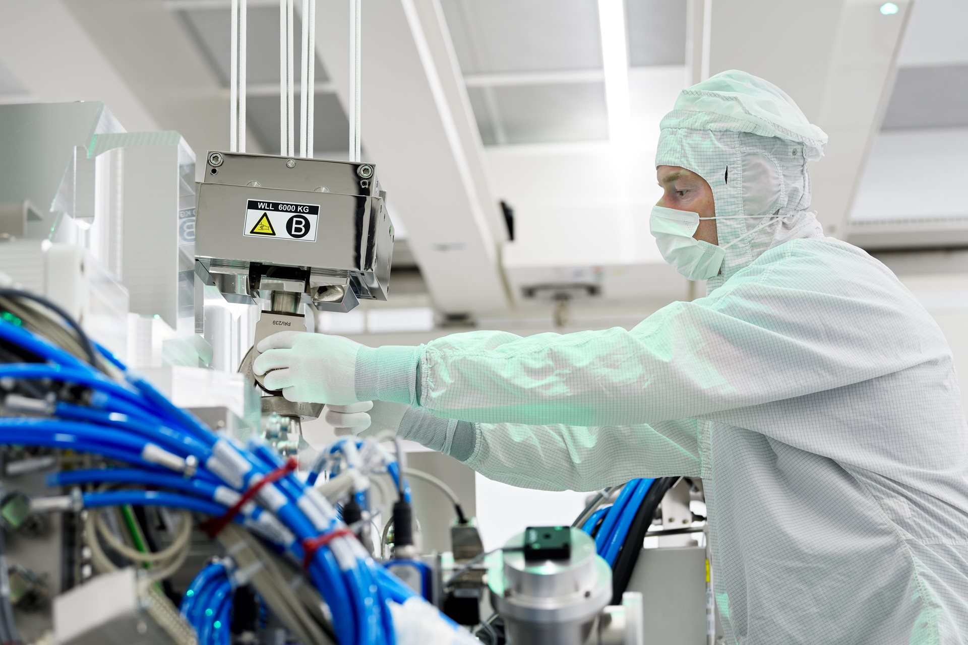
Designed with modular architecture that creates long-term value for the manufacturers, this portfolio of DUV steppers and step-and-scan systems spans i-line, KrF and ArF solutions.
Whether you’re entering a new market, starting a new fab, or scaling up production, this portfolio offers the performance, flexibility, and cost-efficiency needed to meet your business objectives.
Where do you want to make your next breakthrough?
Unrivaled lithography precision for cutting- edge Photonics
Integrated photonics are shaping the future of connectivity with high-speed communication, sensing and data processing. Manufacturing these devices require precise patterning of optical structures and accurate multilayer integration.
ASML’s PAS 5500 systems, such as the /100D, /450F,/850C, and /1150C systems deliver the tight CDU control, capability to handle a variety of wafer sizes & substrates, and excellent overlay accuracies for multi-layer integration, as required by Photonics applications.
Collectively, these features support the flexibility required for diverse photonics applications such as silicon photonics and grating couplers.
Optimized for VCSEL and DFB laser manufacturing
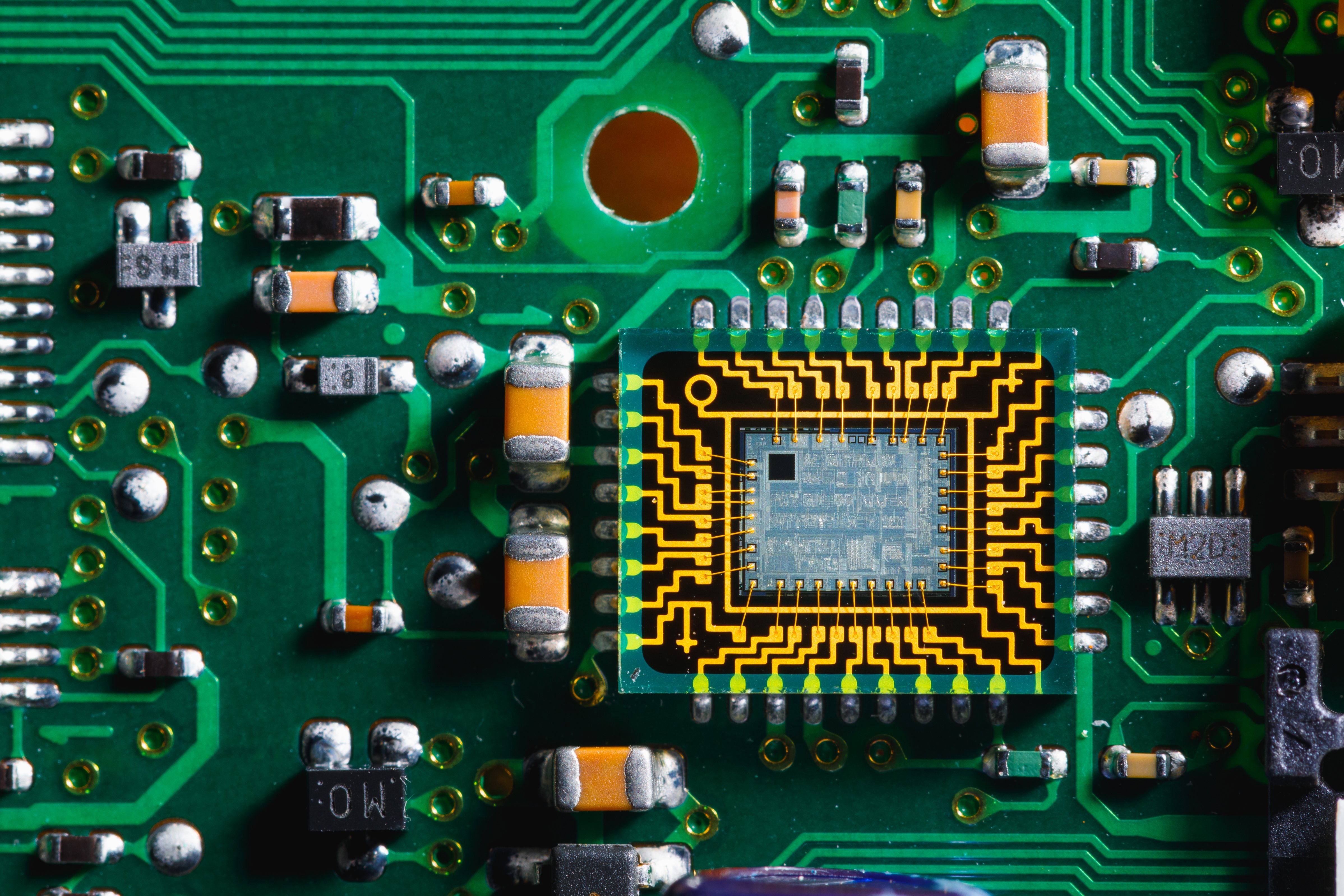
VCSEL fabrication requires critical dimensions in the micron to sub-micron range, are typically fabricated on GaAs substrates, and involve many aligned lithography steps across layers.
The ASML PAS 5500 platform, namely the /275D, /450F, /750F and /1150C, addresses these requirements by combining proven lithography capability, flexibility for specialty substrates, and decades of deployment in compound and advanced semiconductor photonics on small wafer size.
Besides VCSEL, DFB laser manufacturing by e-beam machine as tool-of-record e-beam can also be enabled by PAS 5500 with high productivity and required image performance.
Facilitating Micro-LED Breakthroughs from Lab to Fab
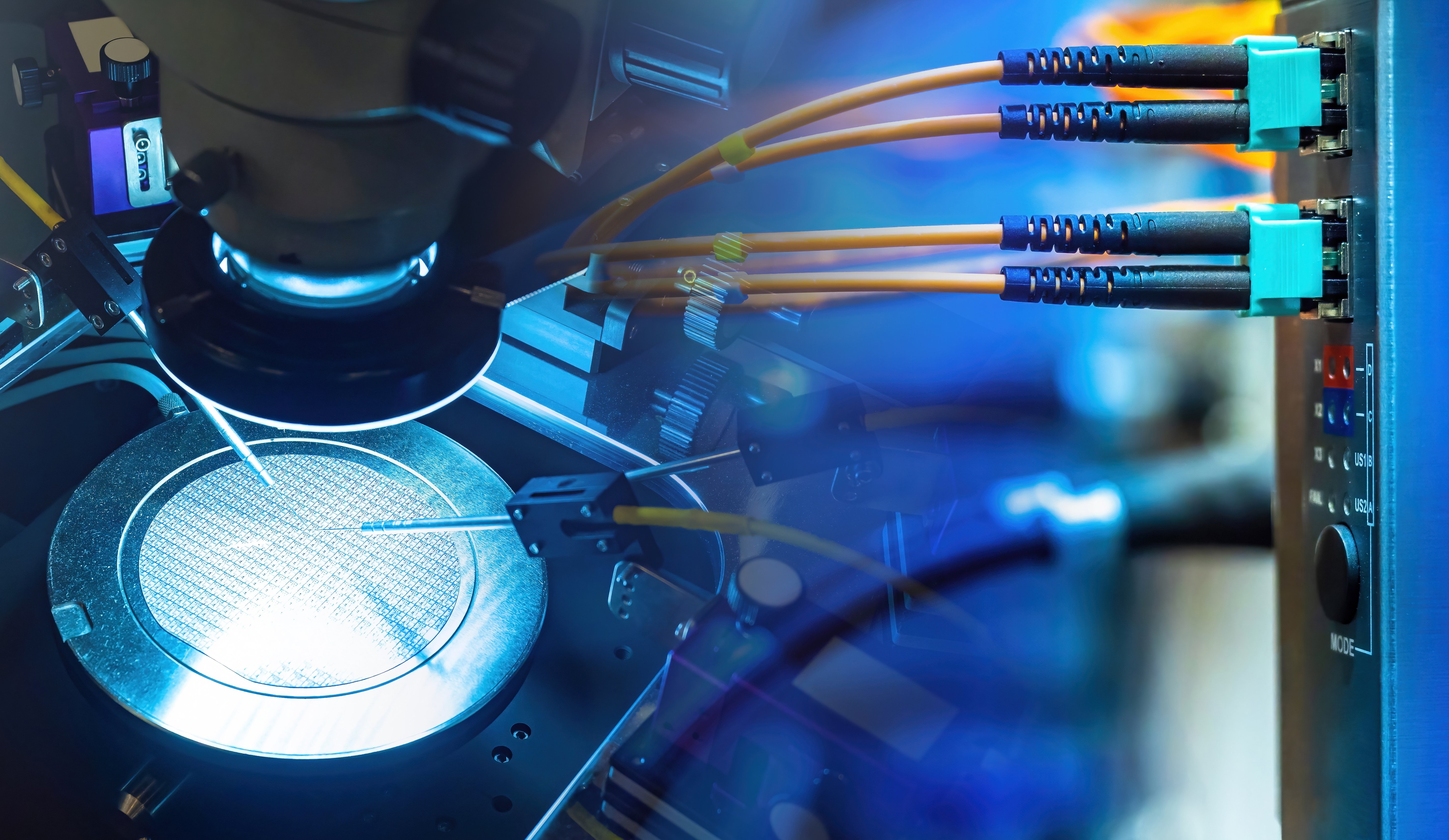
Our PAS 5500 systems such as /100D, /275D and /350C can enable the full spectrum of Micro-LED manufacturing from prototyping to large-scale development.
Precise multi-layer integration and wafer bonding is achievable with Athena (2-color) alignment of multiple layers and Back-side (3D) alignment support.
What’s more? The special wafer handling and wafer edge sensor together support bowed wafers & variety of substrates including glass & sapphire.

Let’s discuss your next breakthrough
Our sales teams are ready to help you explore the right combination of technology, upgrade and service packages for your manufacturing goals
Flexible Solutions for Evolving Power Electronics
PAS 5500 supports a wide range of substrates, including SiC & GaN, and allows for the integration of multi-layer compound devices – features that are critical for modern power electronics.
The platform’s support for thick and thin substrates, as well as bowed wafers make it easier to work with challenging materials and device architectures associated with power devices.
The PAS 5500 portfolio for power electronics include the /100D, /275D, /450F and /850C systems.
Tailored Solutions for MEMS Miniaturization and Scale
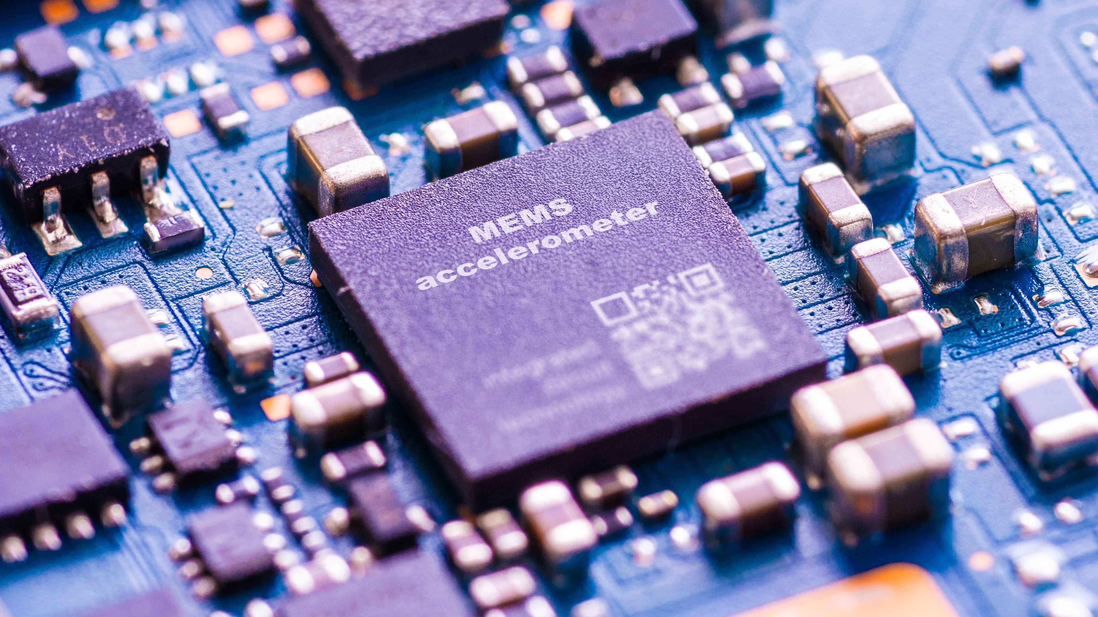
Creating complex, multi-layer MEMS devices demand reliable bonding and integration of intricate MEMS structures.
With its capability to handle small wafers with thick substrates, back-side 3D alignment feature and the excellent overlay packages, PAS 5500 has proven to support both miniaturization and large-scale MEMS production on 200mm wafers while exceeding standard system performance.
The PAS 5500 portfolio for MEMS include the /100D, /275D, /400D and /750F systems.
Accelerating BAW and SAW RF Filter Innovation
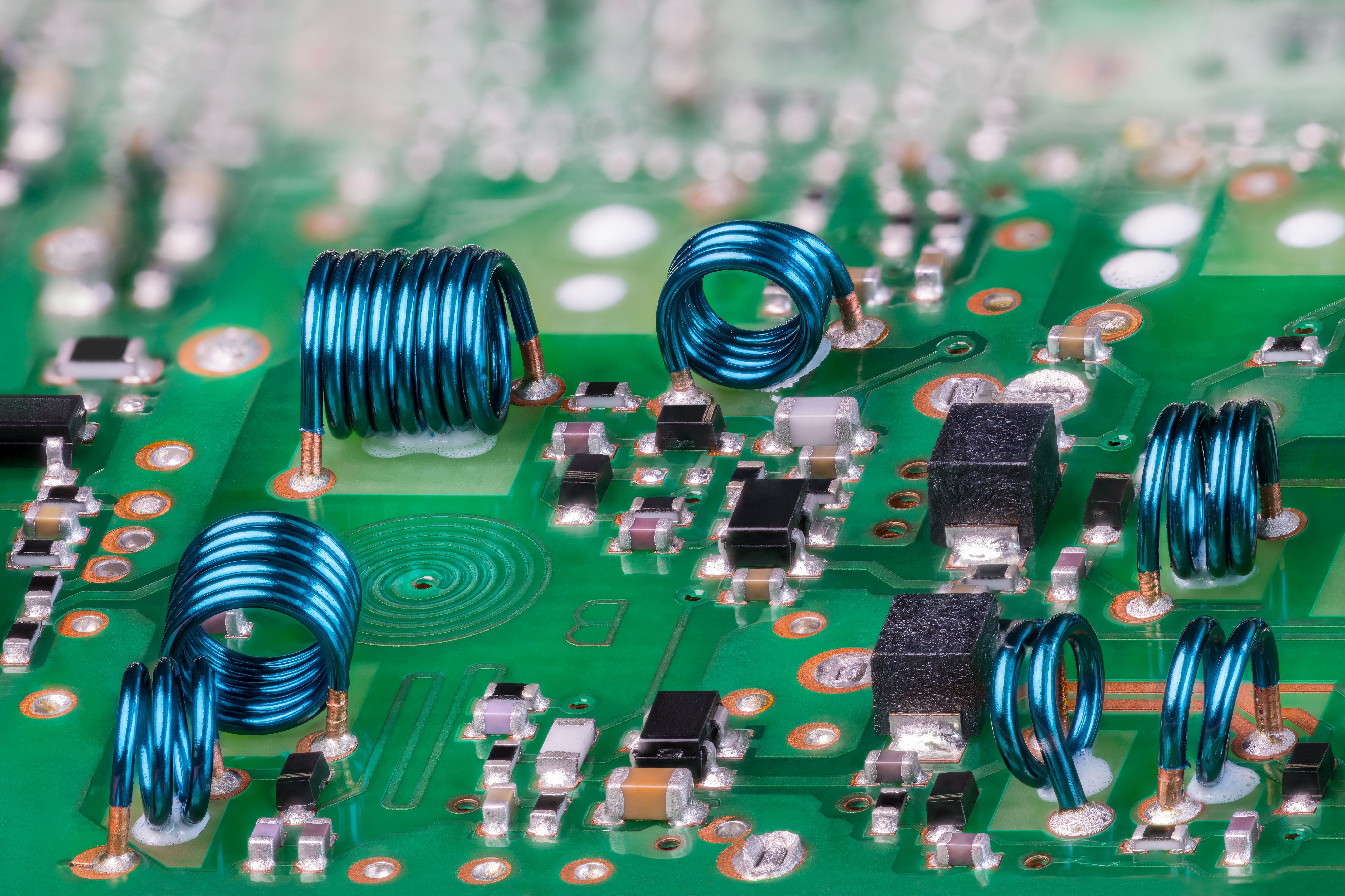
From smartphones and wearable devices to 5G infrastructure, automotive and IoT applications, RF filters require precise acoustic structures that deliver consistent performance at scale.
They require lithography tools that can handle non-standard, thin wafer material such as piezoelectric substrates and offer precise overlay performance, excellent CD control, and drive process stability together with low cost/resonator.
PAS 5500, with its proven mature lithography, delivers exactly this combination which is needed for high-yield BAW and SAW filter manufacturing while maintaining a competitive cost of ownership.
Our PAS 5500 portfolio has a wide range of tools supporting the RF filter innovation, namely /850C, /750F, /450F, /350C,/275D.
Enabling Academic Innovations
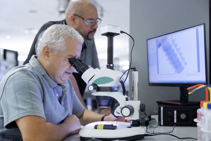
Universities, research institutes and emerging technology teams across the world use mature-node lithography to explore breakthroughs in photonics, sensors, MEMS, power electronics, MicroLED and other specialty applications.
Such institutes often require more than a lithography system. With ASML’s University Service Package, PAS 5500 customers gain access to training, application support, software enhancements and service expertise that help researchers accelerate innovation and move ideas in mature lithography closer to manufacturing reality while keeping operational costs predictable.
Is your Application not listed here?
Power electronics, Sensors, MEMS, Photonics, and MicroLED are just a few of the specialty applications we support. If your innovation requires other specialized lithography capabilities, let's explore how our lithography solutions, applications expertise, and support services can help bring it into production.
Applications engineering for specialty semiconductor manufacturing
At ASML, we don’t just install lithography tools - we partner with you to ensure your unique applications are seamlessly integrated and optimized for excellence.
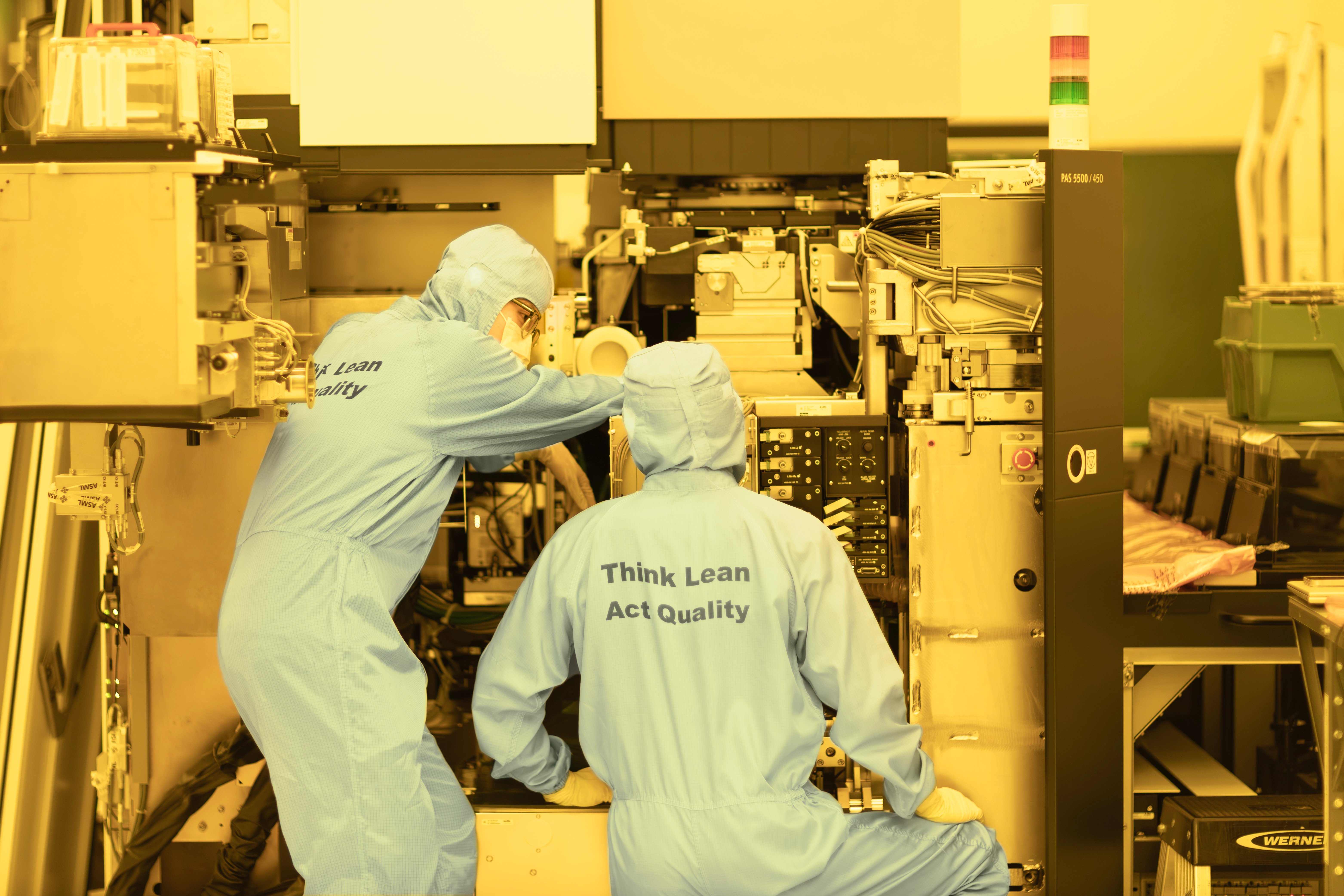
With reliable Install & Qual processes, specialized classroom & on-site trainings, and tailored process-optimization projects, the Applications Support Engineering team ensures that you can overcome process challenges , shorten the pilot run time and boost your manufacturing performance.
Remote support with CARES
Expert support wherever you are
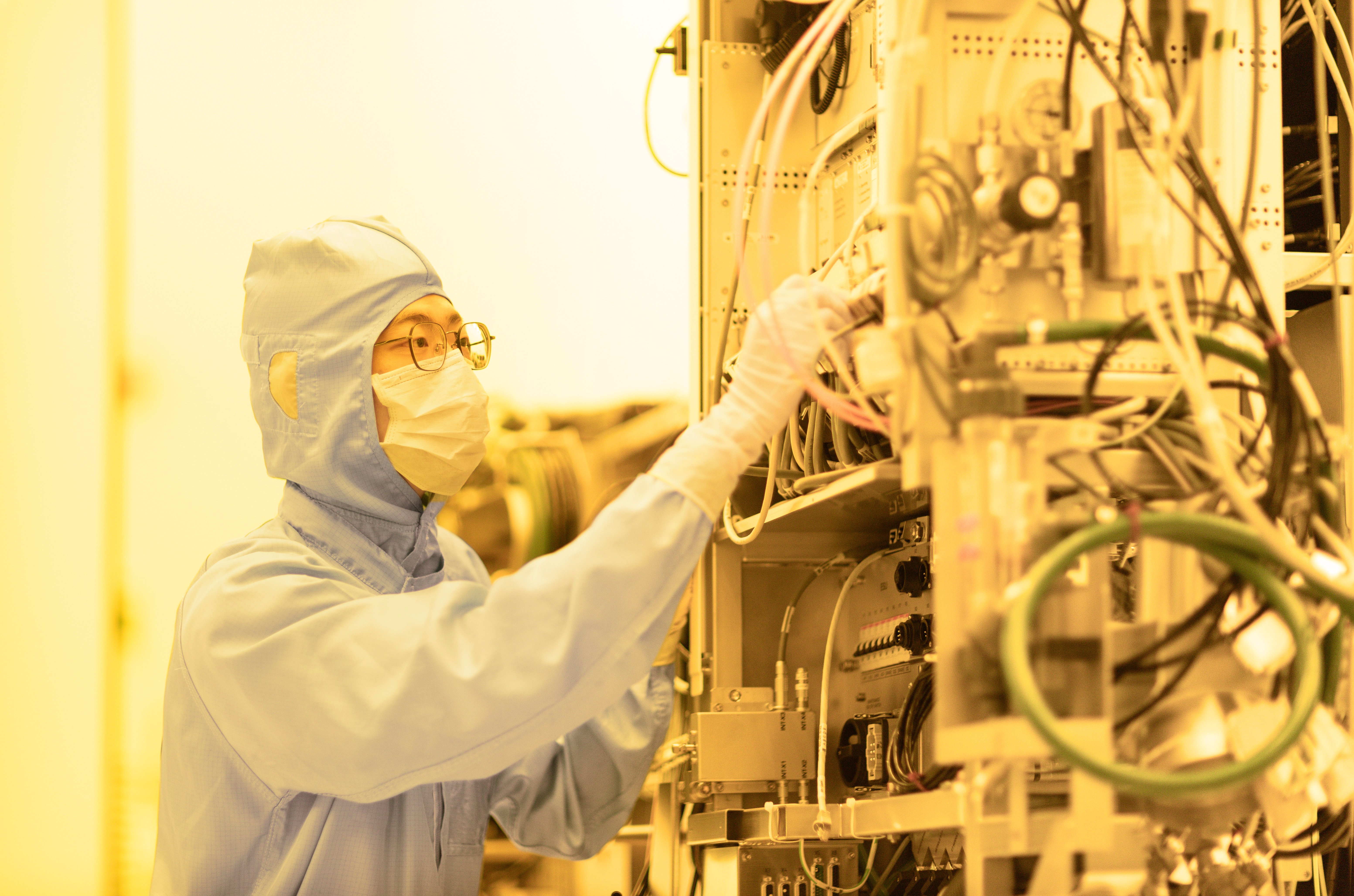
With CARES (Customer Advanced Remote Expert Support), you can get direct and instant access to ASML Engineers’ expert knowledge for real-time troubleshooting with remote support. By combining expert guidance and knowledge sharing, CARES also accelerates your team’s skill development, enabling your engineers to resolve issues faster and more independently.
The Result?
Minimized downtime, optimized fab performance, and reduced environmental impact with less travel.

Let’s discuss your next breakthrough
Our sales teams are ready to help you explore the right combination of technology, upgrade and service packages for your manufacturing goals