
Using lithography with shorter wavelengths of light and more powerful optical systems enables smaller, denser and more powerful microchips.
The last part of the Rayleigh equation is a coefficient known as the ‘k1-factor’, which is a collection of everything else that we can do in the lithography process to enhance the resolution of our systems. The key is pushing our systems closer and closer to k1’s physical limit.
Controlling light
Controlling how light hits the reticle has a big impact on k1 and the resolution. Inside the lithography system, the illuminator collects and focuses light from the source onto the reticle, and can implement various techniques to give chipmakers better control over their lithography process and improve performance without affecting the system’s speed. For example, off-axis illumination shines light onto the reticle at an angle to better control how the light diffracts from the pattern. Similarly, shaping the beam into different ‘pupil shapes’ ranging from simple spots to complex patterns of dots can control how the light interacts inside the system to improve the contrast of the image.
Getting pupils into shape
As chip features become smaller, pupil shapes are becoming more complex and tailored to get the optimal resolution out of the light. In the past, diffractive optical elements (DOE) to create the desired pupil shape would be manually inserted into the illuminator to get the best possible result. But in our industry, time is money. In today’s ASML DUV systems, the FlexRay free-form illuminator features an array of 4,000 individually controllable mirrors that, together, can instantaneously create any pupil shape you can imagine. In our EUV systems, the FlexPupil free-form illuminator fulfills a similar role.
Simulating the best blueprint
Using the vast amounts of data generated by our systems, computational lithography simulates the manufacturing process with powerful algorithms. These simulations help to design a chip blueprint (the reticle) that contains the pattern to be printed on the wafer. That’s how we make sure that our lithography machines print what they should. This technique is called optical proximity correction (OPC) and is often combined with specific illumination optimizations in the lithography system.
LITHOGRAPHY PRINCIPLES
The science behind the chip The Rayleigh criterion
Read more
Learn the equation that determines just how small the transistors on a microchip can be.
 Light & lasers
Read more
From visible blue light to invisible extreme UV light, our lithography machines keep innovation in light and lasers moving forward.
 Lenses & mirrors
Read more
The complex optical systems in our lithography machines reduce the image to be printed on a wafer to the nanometer level.
 Mechanics & mechatronics
Read more
Our lithography machines feature some of the world’s most advanced, precision-engineered mechanical and mechatronic systems.
 Measuring accuracy
Read more
ASML systems rely on data from sensors as well as diffraction-based and electron beam measurements to optimize chip production.
More about ASML technology
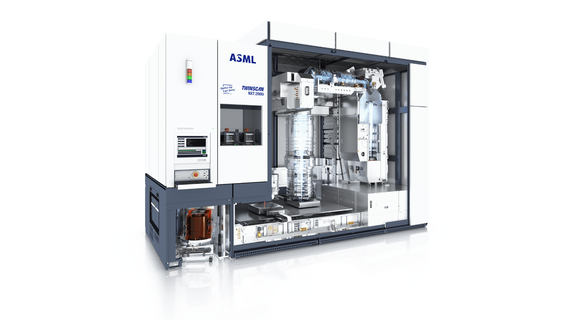
 EUV lithography systems
Providing highest resolution in high-volume manufacturing, ASML’s extreme ultraviolet lithography machines are pushing Moore’s Law forward.
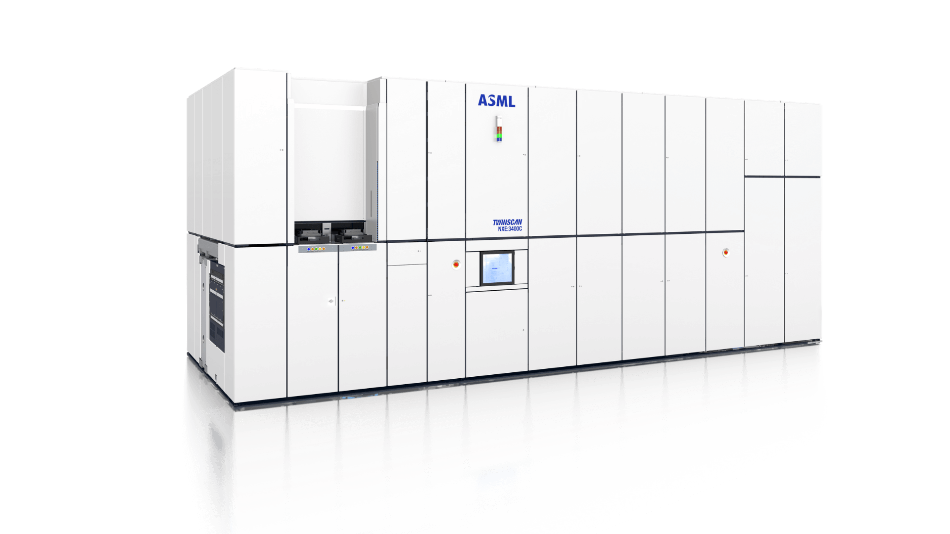
 DUV lithography systems
ASML's deep ultraviolet (DUV) lithography systems dive deep into the UV spectrum to print the tiny features that form the basis of the microchip.
Metrology and inspection systemsDelivering speed and accuracy, our metrology and inspection portfolio covers every step manufacturing processes, from R&D to mass production.
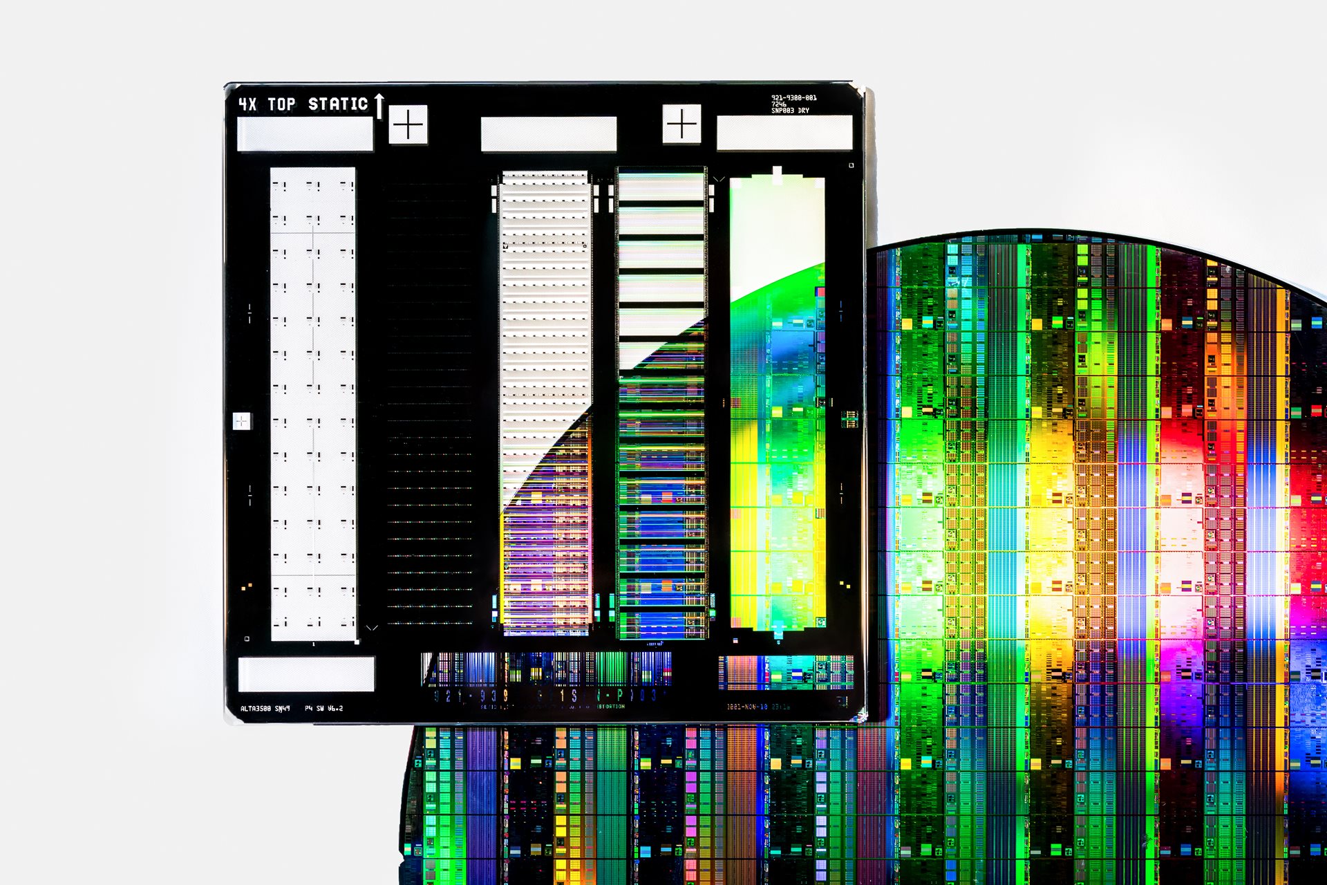 Computational lithography
ASML's industry-leading computational lithography products enable accurate lithography simulations that help to improve chip yield and quality.