Chipmakers use our products to print chip patterns and inspect those patterns using advanced metrology systems and software, allowing them to increase accuracy and yield.
Types of metrology and inspection
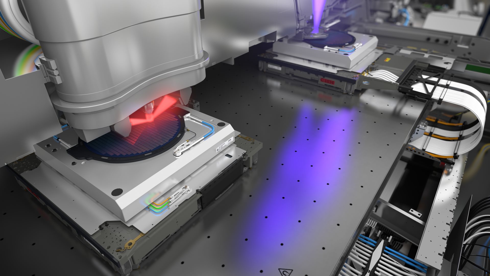
There are two ways to examine the quality of the printed features on a chip: diffraction-based optical measurement and e-beam inspection.
Diffraction examines how light reflects from the wafer, while e-beam observes how electrons scatter when they come into contact with the wafer.
ASML uses both: our YieldStar systems use diffraction-based measuring to assess the pattern quality on the wafer, and HMI e-beam inspection systems help locate and analyze individual chip defects.
Combined with sensor-based information from inside our lithography machines and a complex set of software algorithms, the YieldStar and HMI systems provide a wealth of data that chipmakers use to optimize their manufacturing process.
Optical metrology
YieldStar
ASML's YieldStar systems do just what their name suggests: they help our customers increase their yield, or the proportion of functioning chips on the wafer. YieldStar allows manufacturers to track key production parameters such as overlay (the accuracy with which two layers of a chip are aligned). Our YieldStar systems are usually integrated into the production line so that they can measure quickly and accurately, looping the data back to the lithography system for real-time corrections to the manufacturing process.

How it works
E-beam metrology and inspection
HMI e-beam solutions
For today’s advanced microchips, defects as small as a couple of nanometers can render the entire chip useless. With its 1-nanometer resolution, e-beam inspection offers just the right kind of eyes to spot those tiny misprints.
ASML is at the forefront of developments in e-beam metrology and inspection. E-beam achieves a higher resolution than YieldStar, but it measures more slowly, which means that it’s typically used after the pattern is etched onto the wafer.

How it works

In-scanner metrology
Precision and speed are paramount for today’s advanced chipmaking machines. But sub-nanometer inaccuracies inevitably creep in due to material imperfections, temperature fluctuations and atmospheric pressure changes. Scanner metrology software uses computational models of machine processes in machines to predict and coordinate how the powerful mechatronic modules within our lithography systems should behave to compensate for physical imperfections and maximize system performance.
Read more
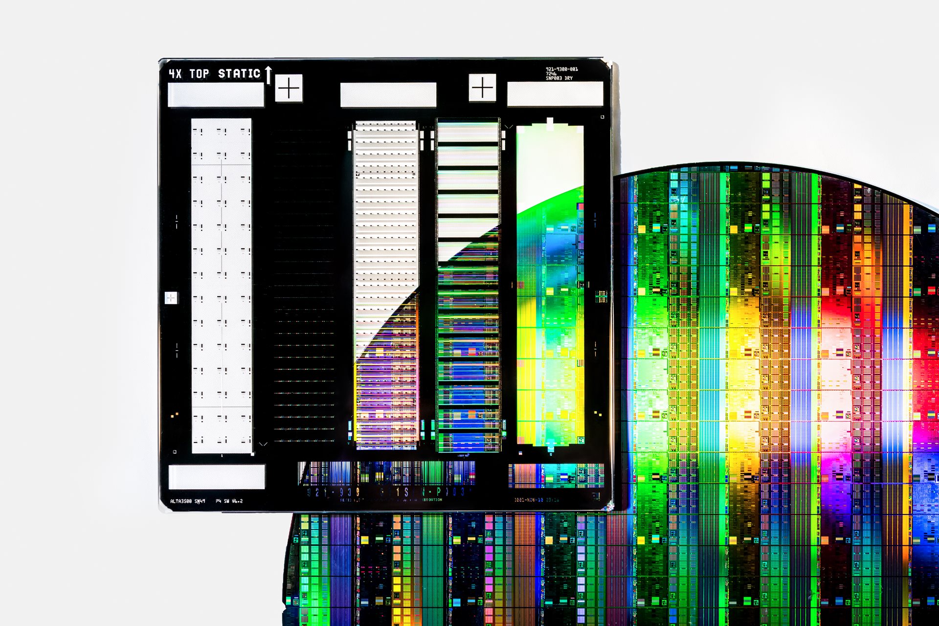
Pattern fidelity
Pattern fidelity control (PFC) is a new paradigm in chip manufacturing, aiming to deliver the full benefits of our holistic lithography approach. By drawing and analyzing the most precise data from a wider range of sources throughout the entire chip development and manufacturing process, it gives chipmakers unprecedented insights into the patterns they are actually printing on wafers. Powerful algorithms then translate those insights into actions. These actions are implemented in the lithography system to prevent pattern defects and enable high yields, even when producing the most complex chips.

Read more
Lithography principle
The science behind the chip The Rayleigh criterion
Read more
The equation that determines just how small the features on a microchip can be.
 Light & lasers
Read more
Our lithography machines keep innovation in light and lasers moving forward.
 Lenses & mirrors
Read more
Learn about the role of lenses and mirrors in ASML’s lithography machines.
 Mechanics and mechatronics
Read more
Speed and precision meet in ASML’s advanced lithography machines.
 Pushing 1k further
Read more
ASML is pushing fundamental physical concepts to their absolute limit.
More about ASML technology
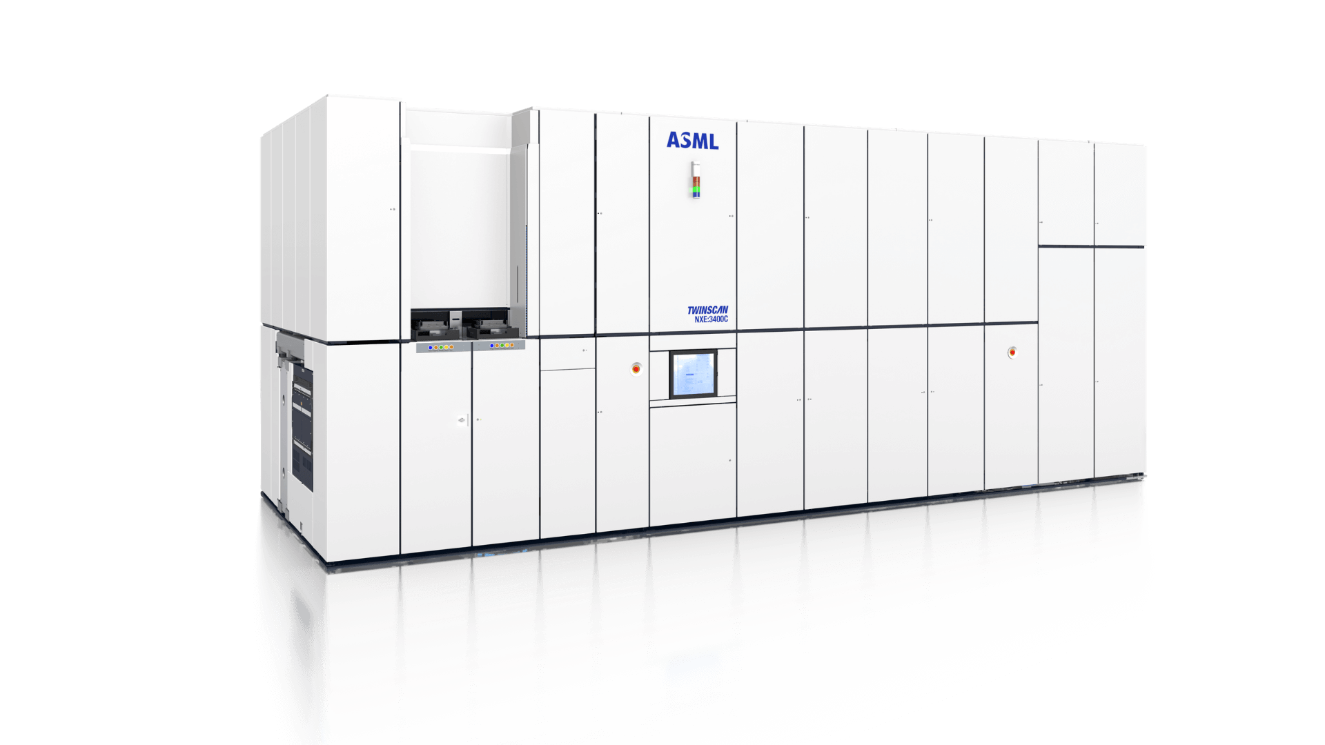 EUV lithography systems
Providing highest resolution in high-volume manufacturing, ASML’s extreme ultraviolet lithography machines are pushing Moore’s Law forward.
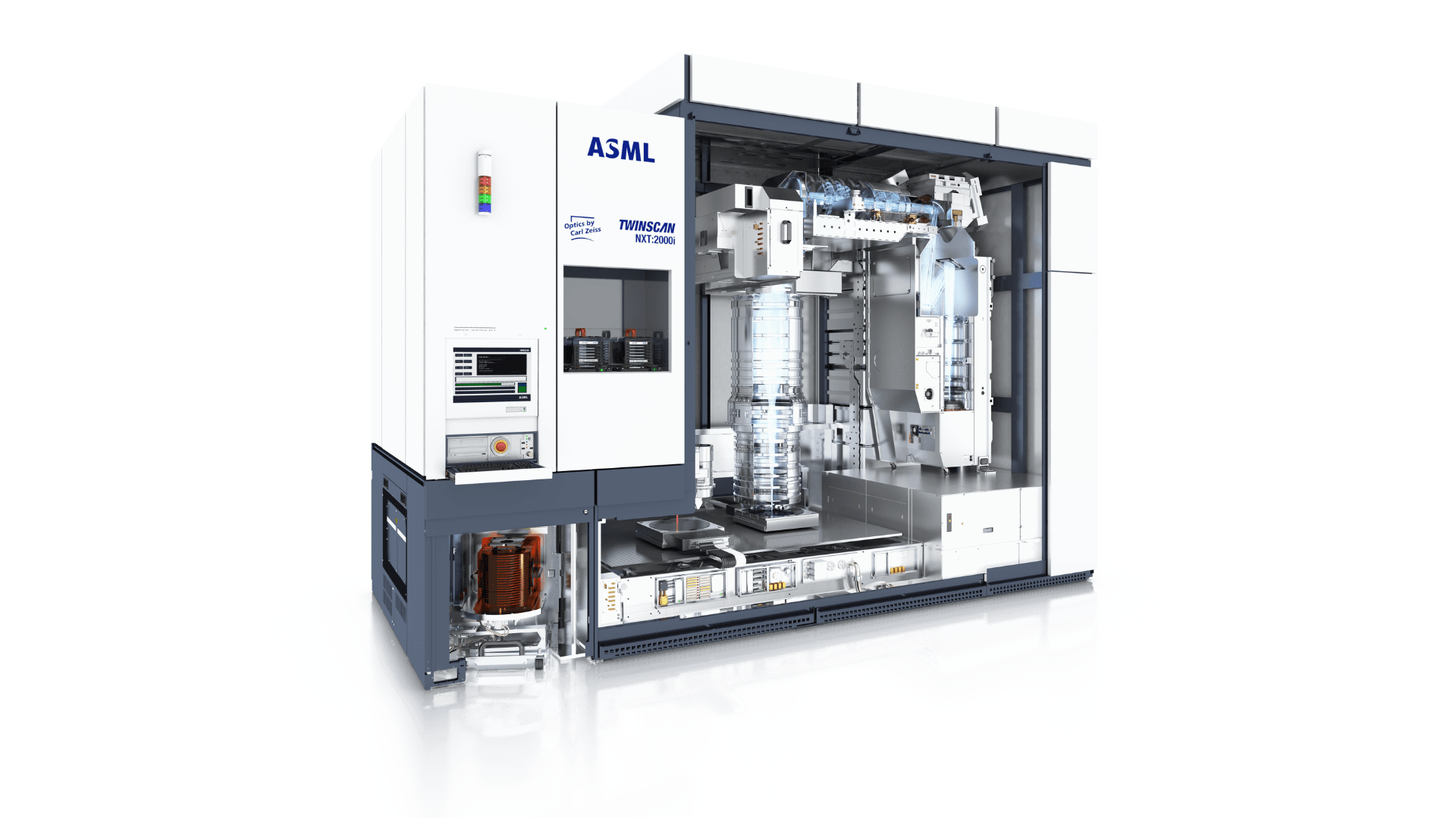 DUV lithography systems
ASML's deep ultraviolet (DUV) lithography systems dive deep into the UV spectrum to print the tiny features that form the basis of the microchip.
 Metrology and inspection systems
Delivering speed and accuracy, our metrology and inspection portfolio covers every step manufacturing processes, from R&D to mass production.
 Computational lithography
ASML's industry-leading computational lithography products enable accurate lithography simulations that help to improve chip yield and quality.