We developed computational lithography as part of our ASML product portfolio to provide the production yields and performance our customers demand when working on the nanoscale.
Without computational lithography, it would be impossible for chipmakers to manufacture the latest technology nodes.
The smaller the scale, the bigger the problems
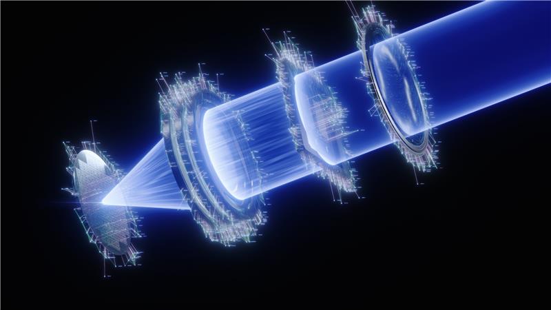
During lithography, diffraction of the light as well as physical and chemical effects in the photosensitive layer deform the image the machine is trying to print (think of this as trying to draw a thin fine line with a broad watercolor paint brush - it smudges in many places).
With the introduction of 130 nm technology, addressing these deformations became essential to prevent defects. As chipmakers continued to shrink the patterns to make small and more powerful chips, the problems and complexity escalated, requiring ever-more sophisticated approaches.
Model manufacturing
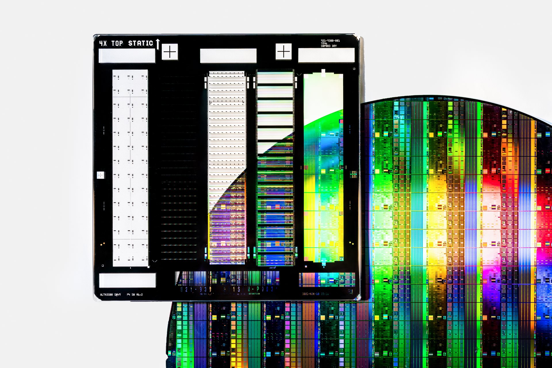
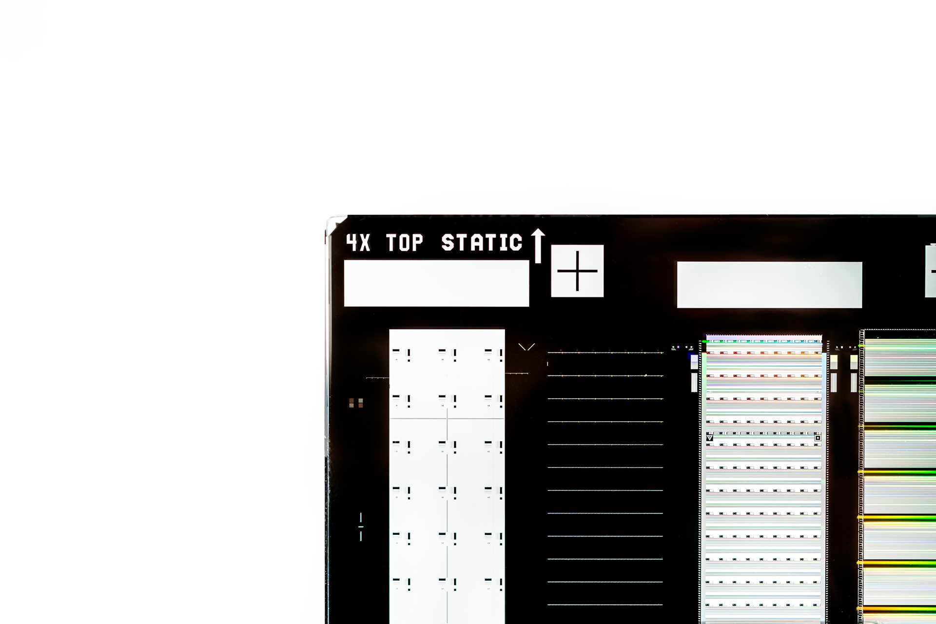
Computational lithography uses algorithmic models of the manufacturing process, calibrated with key data from our machines and from test wafers. These models are used to optimize the mask, or blueprint of the desired end result, by intentionally deforming the patterns to compensate for the physical and chemical effects that occur during lithography and patterning. The net result: we end up with an accurate replica of the desired chip patterns on the wafer.
Computational power
Whereas others look ‘upstream’ towards chip design, ASML looks ‘downstream’ towards manufacturing to distinguish our market position. Computational lithography has not only been instrumental to the continued scaling of the world’s semiconductor devices but also to the increasing performance of our machines.
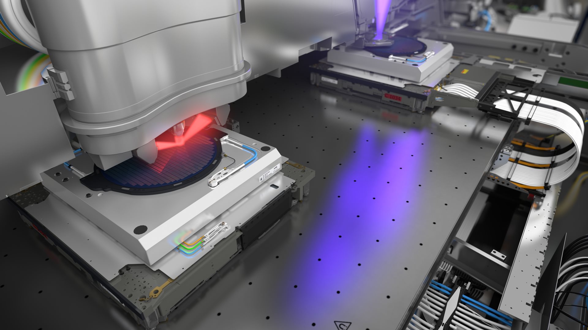
Our computational lithography techniques optimize the scanner, masks and processes for device manufacturability and yield, both early in design and technology development and later in high-volume production.
Beyond Moore’s Law
As technology advances and wafer patterns shrink, the requirements for accuracy in our models increase. Today in high-volume manufacturing we’re imaging features down to the single-nanometer level, with (for simple 1D features) sub-nanometer accuracy requirements.
Going forward, computational lithography will continue to play an indispensable role in improving the imaging performance of our machines, allowing us to continue driving Moore’s Law forward.
Holistic printing
We’re expanding the power of computation from lithography alone to optical metrology and e-beam inspection, as well as machine learning applications. We continue to develop modeling and correction software suites to link our metrology and inspection systems with our lithography systems, leveraging our expertise in both fields.
