ASML receives order for its most advanced 150 nm lithography tools

Order from White Oak Semiconductor

Press release - Tempe, Arizona, December 7, 1999

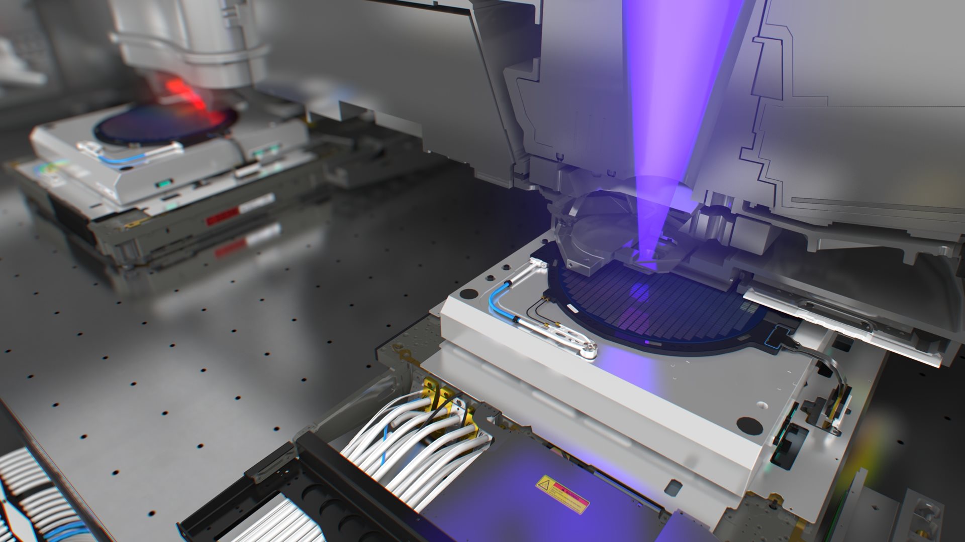
To increase its manufacturing capacity in advanced semiconductor devices, White Oak Semiconductor has placed an order with ASM Lithography (ASML) for multiple PAS 5500/700 deep UV Step & Scan systems. The lithography tools are being installed in White Oak's wafer fab in Richmond, Virginia. ASML's PAS 5500/700 product is designed for 150 nm design rule applications with a production throughput of 104 200 mm wafers per hour. Introduced in October 1998, it is the world's first production-worthy system for 150 nm lithography, combining the industry's fastest scanning stages with the highest numerical aperture (NA) lens, capable of a 0.70 NA.

About White Oak Semiconductor


White Oak Semiconductor employs 1,500 people at the world headquarters located on 210 acres in the White Oak Technology Park near Richmond, Virginia. The high-volume semiconductor site is fully integrated with wafer manufacturing, probe, assembly, and final component testing as well as final DIMM-module assembly and test, all performed at the 800,000-square-foot facility.

About ASML


ASM Lithography was founded in 1984 and is a world leader in advanced photolithography systems that are essential to the fabrication of modern integrated circuits. ASML is publicly traded on both the Amsterdam Exchanges and on the Nasdaq Stock Market under the symbol ASML. Visit the company's website at www.asml.com for more information.

Contact information

  • Brittney Wolff Zatezalo
  • Corporate communications manager US
  • +14084833207