Press release - Murray Hill, New Jersey, November 3, 1999
A group of semiconductor device and equipment manufacturers today announced a joint agreement aimed at accelerating the development of SCALPEL technology into a production lithography solution for building future generations of integrated circuits. Participants in the program include eLithTM LLC, a joint venture of Applied Materials Inc. and ASM Lithography Holding NV; Lucent Technologies Inc.; Motorola Semiconductor Products Sector; Samsung Electronics Co. Ltd.; and Texas Instruments Incorporated (TI). The program will remain open to additional companies interested in furthering this technology.
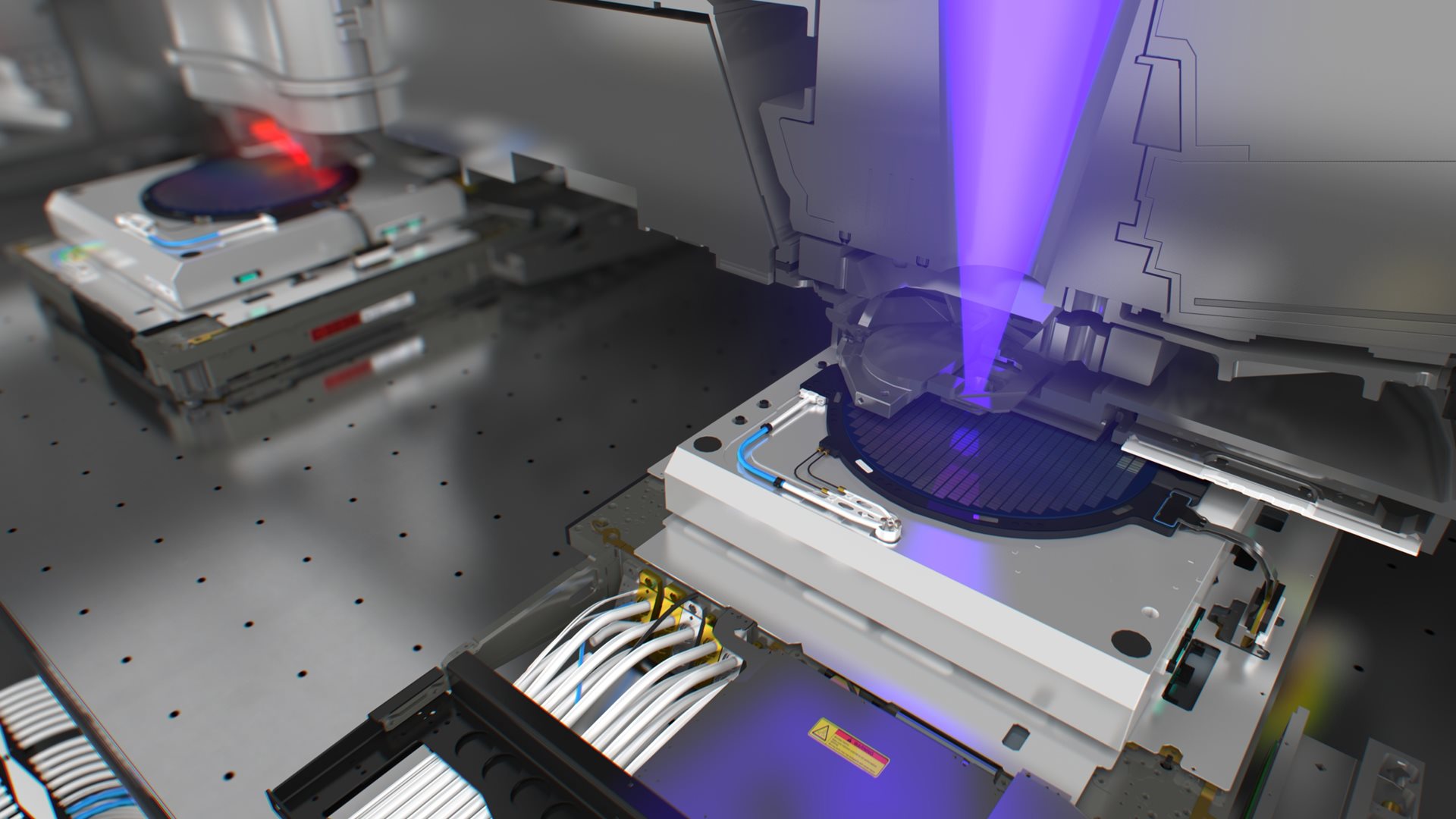
SCALPEL projection electron lithography is being developed as a potential successor to current optical lithography methods for patterning smaller, more powerful chips. Using an electron source instead of a light source, projection electron technology has the capability to print images with features smaller than 50 nanometers (0.05 micron), compared to today's leading-edge 180 nanometers (0.18 micron) technology.
"Motorola is pleased to be part of this group of leading-edge companies which will assure that SCALPEL technology is vigorously pursued," said Joe Mogab, manager of Advanced Process Development for Motorola's DigitalDNA Laboratories. "We feel that SCALPEL can become a strong technology for next generation wafer processing which will help us maintain our leadership in embedded processors."
"We are delighted to be part of the effort to explore this exciting new area of lithography," said Dr. Moon Yong Lee, senior vice president of the Semiconductor R&D Center for Samsung. "Projection electron lithography has already shown significant potential to be the technology of choice to create the circuits that will be needed for advanced DRAMs (dynamic random access memory) as we move to 0.1 micron geometries and beyond."
Dr. Bob Helms, vice president and director of Silicon Technology Research of Texas Instruments said, "TI is pleased to facilitate the commercialization of electron projection lithography through participation in this program. We believe this advanced lithography approach has the greatest potential for our DSP and ASIC market segments in terms of high wafer volume and low cost of ownership. The continuation of this development effort can potentially reduce semiconductor manufacturers costs and continue technology development at the 100 nm (0.1 micron) node and beyond."
"The industry leaders who have joined this program validate our belief that SCALPEL technology, developed at Lucent's Bell Labs, is the most promising route to ICs with 0.1 micron and smaller feature sizes," said Mark Pinto, chief technical officer of Lucent Technologies Microelectronics Group. "This agreement will help accelerate the realization of commercially viable systems that will allow us to deliver future generations of communications networks and handheld devices."
To facilitate working on the program, equipment manufacturers Applied Materials and ASM Lithography have formed a joint venture, eLith LLC. "The ultimate goal of this venture is to commercialize electron projection technology as a production-worthy manufacturing tool to enable the migration of chip technology and the continuation of Moore's Law," said Dr. Sass Somekh, senior vice president of Applied Materials. "We are excited to be involved with several of the industry's top semiconductor manufacturers who are supporting this effort."
Martin van den Brink, ASML executive vice president of Marketing & Technology, added, "The program offers us an excellent opportunity to work directly with end-users to develop one of the solutions that may be integrated into future manufacturing lines. Our participation in this collaborative effort, which is part of our advanced lithography roadmap activities, affords us an opportunity to contribute our expertise in advanced imaging systems to further the development of electron projection lithography."
About the companies


