Press release - Munich, Germany, April 4, 2000
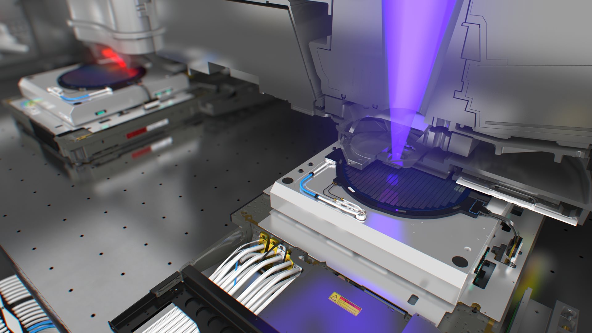
ASML has announced the semiconductor industry's first KrF (248 nm wavelength) lithography system optimized for high-volume production of ICs with 130 nm design rules. The new PAS 5500/750E deep ultraviolet (UV) Step & Scan tool, introduced here at the annual SEMICON Europa trade show, provides a complete process solution by delivering significant improvements in imaging, overlay and productivity.
"This new tool allows IC makers to bring their most advanced product designs, such as 4-gigabit memory devices and gigahertz-speed logic chips, from R&D into mass production using proven, economical 248 nm lithography," said Paul van Attekum, ASML vice president of product marketing. "We have raised the performance bar across the board for production-worthy lithography equipment."
Semiconductor manufacturers are reaching the point where 130 nm resolution is needed in production to continue shrinking device feature sizes. Leading-edge DRAM, logic IC manufacturers and IC foundries are already developing processes for 130 nm lithography, but they need a production-ready exposure system. ASML's new PAS 5500/750E achieves 130 nm resolution while using standard 248 nm light, the most economical choice based on illumination cost, resist maturity, process experience and overall cost of ownership. The scanner features the Starlith 750 lens, Carl Zeiss newest deep UV lens with an unrivaled numerical aperture (0.7), the highest partial coherence (0.88), and the lowest aberrations available today.
To optimize process latitude for 130 nm imaging, the PAS 5500/750E is equipped with ASML's AERIAL II illuminator, which provides high intensity for both conventional and annular illumination. In addition, the tool includes as standard the QUASAR module, which enables multipole illumination. Designed as an extension of the AERIAL II illuminator, QUASAR allows IC makers to optimize their depth of focus and exposure latitude process window and reduce mask error factors for the most advanced layers of circuitry. The multipole illumination mode is generated optically, maintaining exposure intensity for maximum productivity. The PAS 5500/750E delivers the industry's tightest overlay at less than 30 nm, as required for producing semiconductor devices with 130 nm design rules.
The new ATHENA dual-wavelength, high-order alignment system is also included as standard for increasing the alignment process latitude on today's most advanced process layers such as tungsten CMP. A 2 kHz, 20 W laser and high-transmission optics provide 2,400 mW/cm2 of exposure intensity at the wafer plane. Combined with low alignment overhead and high-speed scanning stages, this allows the PAS 5500/750E to deliver industry-leading throughput of 120 200 mm wafer per hour at realistic production conditions of 50 mJ/cm2 and 46 exposures fields. Lasers may be selected from among multiple suppliers and will support variable laser frequency control for lower cost of ownership. The first shipments of this product are scheduled to begin in the second quarter of this year.
About ASML
Forward-looking statements


