Press release - Veldhoven, The Netherlands, January 31, 2001
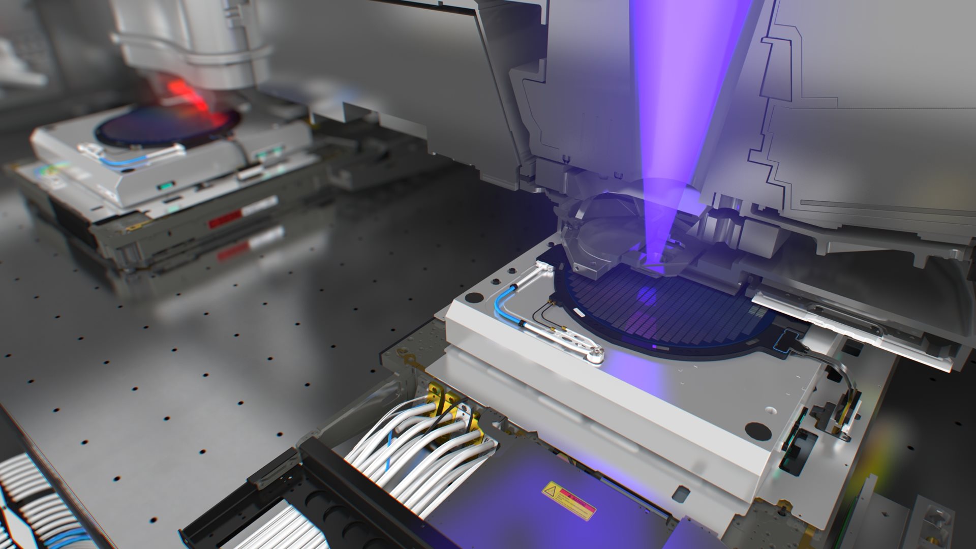
Extending mature, cost-effective KrF (248 nm wavelength) lithography for volume production applications at 120 nm resolution and beyond, ASML today introduced its newest deep UV Step & Scan system, the PAS 5500/800. The system achieves 120 nm resolution by means of the industry-leading numerical aperture (NA) of 0.80. With throughput of 115 200 mm wafers per hour, this product is designed for high-volume processing of today's most advanced ICs as well as R&D applications for next-generation products.
The PAS 5500/800 Step & Scan system incorporates the new Starlith 800 lens from Carl Zeiss, ASML's optics partner. Advanced illumination options will be available building upon ASML's unique advanced AERIAL II illuminator design, and offering greater flexibility to increase contrast for pattern-specific applications as the industry migrates to low k1 imaging in production. The PAS 5500/800's lens design, improved with lower aberrations, allows ASML's customers to shrink IC design rules and to leverage their experience with KrF manufacturing technology.
"The new PAS 5500/800 system increases our leading-edge customer's competitive advantage and profitability by extending the life of existing KrF technology using mature photoresists and processes," said Martin van den Brink, ASML's executive vice president for marketing and technology. "This new product's versatility makes it one of the most cost-effective and high-performance imaging systems available today."
The system features ASML's patented ATHENA wafer alignment system in combination with reticle alignment using the actinic wavelength (Reticle Blue Alignment), enabling industry leading overlay accuracy of 20 nm in a single machine and 30 nm from machine to machine. In addition, a new wafer-leveling system substantially enhances the leveling process latitude, resulting in focus margin improvement. Using ASML's stable PAS 5500 system architecture, the new product is readily field compatible with customers current installed bases of ASML deep UV and i-line equipment. In fact, the PAS 5500/800 matches seamlessly with the PAS 5500/400C i-line scanner, which further improves cost efficiencies through the use of mix-and-match manufacturing strategies. The first production units of the new PAS 5500/800 system are scheduled to begin shipping in June 2001.
About ASML


