Press release - Veldhoven, the Netherlands, July 9, 2001
ASML Holding NV today announced the industry's first high-productivity, dual-stage ArF (193 nm) lithography system for 300 mm wafer processing with 100 nm resolution. Developed for volume production applications, the new AT:1100 is a 193 nm wavelength system with the industry's highest numerical aperture ArF lens (NA=0.75). These systems, which will be delivered to customers in the fourth quarter of this year, build upon ASML's successful 300 mm TWINSCAN dual-stage platform introduced in July 2000.
"We have already received several orders from new and existing ASML customers, and expect to ship the first AT:1100 in the next six months, demonstrating ASML's commitment to anticipating and meeting customer demand for leading-edge imaging technology," said Martin van den Brink, executive vice president of marketing and technology for ASML. "In line with the accelerated SIA roadmap, this exciting and challenging ArF technology will provide for the volume production of microprocessors with more than 75 million transistors and thereby enable a whole new generation of microelectronic products and applications."
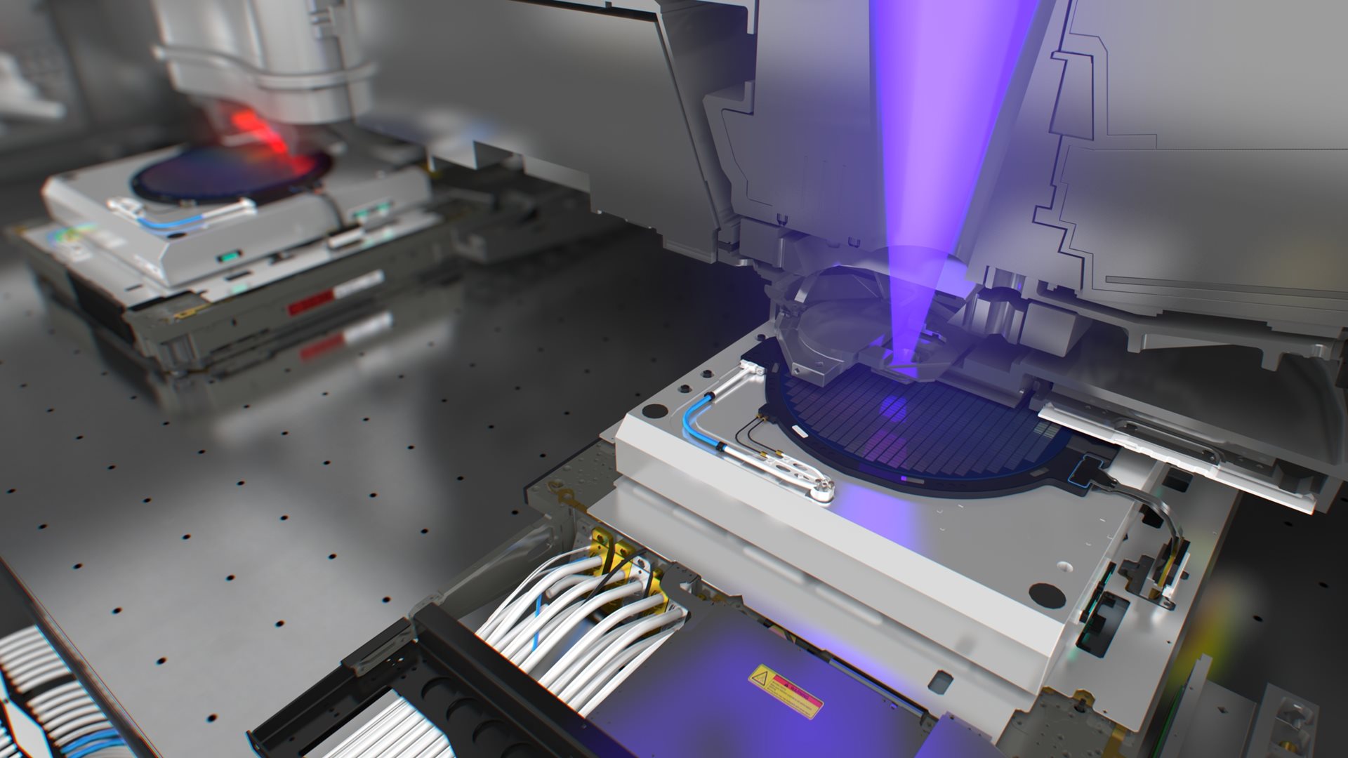
The system incorporates a second-generation ArF, 0.75 NA StarLith 1100 lens from ASML's optics partner, Carl Zeiss. The 193 nm lens offers the highest NA available today in an ArF system. The StarLith's improved aberration control reduces influence on critical lithography structures, which enhances the imaging performance. The 193 nm wavelength system extends optical lithography to the 100 nm node and beyond using cost-effective binary photomasks, which enable chip manufacturers to continue using mature photomask technology for critical levels instead of migrating to more expensive (phase shift) masks. TWINSCAN's dual wafer stage technology enables the exposure of one wafer and the alignment of the next wafer to take place in parallel. When imaging is completed on a wafer, the two stages are exchanged and the pre-aligned wafer moves into the exposure position. This virtually eliminates overhead time and allows continuous patterning of wafers for maximum productivity.
The AT:1100 achieves a throughput of 93 wafers-per-hour at a dose of 20 mJ/cm2. By separating the align and expose operations, more extensive and accurate alignment and wafer surface height mapping of the entire 300 mm wafer can be performed without impacting throughput. This increase in metrology accuracy is essential for delivering the 100 nm critical dimension control and less than 20 nm overlay across the wafer at full throughput. The AT:1100 introduces new 4 kHz ArF laser technology which contribute to its leading productivity advantage. The AT:1100 is designed for seamless mix-and-match operation with ASML's TWINSCAN product family, including the AT:750, a 248 nm deep UV system, and the AT:400, an i-line system, thereby ensuring the lowest cost per level even with advanced process technologies. The TWINSCAN platform allows either left- or right-hand configuration for optimum fab layout with track processing equipment and 300 mm automated materials handling systems. The modular design reduces system installation time for faster fab ramp up and time to market for advanced chips. A scale model and multimedia presentation of the AT:1100 and TWINSCAN technology platform will be displayed at SEMICON West 2001, being held July 16–18 at the Moscone Center in San Francisco (South Hall, Booth #2226).
About ASML
Forward-looking statements


