Press release - Veldhoven, The Netherlands, November 27, 2001
ASML Holding NV of the Netherlands (ASML) today announced that it will converge its 193 nm wavelength product offering onto a single platform, the TWINSCAN AT:1100, the industry's first high-productivity, dual-stage ArF (193 nm) lithography system for 300 mm wafer processing with 100 nm resolution.
ASML will discontinue before year-end the development and shipment of its Micrascan V product, a 193 nm wavelength system acquired through the company's merger in May 2001 with the Silicon Valley Group, Inc. The company will extend TWINSCAN manufacturing competencies and certain R&D programs from the Netherlands to the Wilton, Connecticut, facility to optimize ASML's industrial base in the United States.
Doug Dunn, ASML's President and CEO, said: "Our decision was made after close consultation with customers and we expect to ship our TWINSCAN AT:1100 product in early 2002 as a result of that. It is very important for ASML to concentrate our talent and leading edge technology on one platform, the industry standard TWINSCAN."
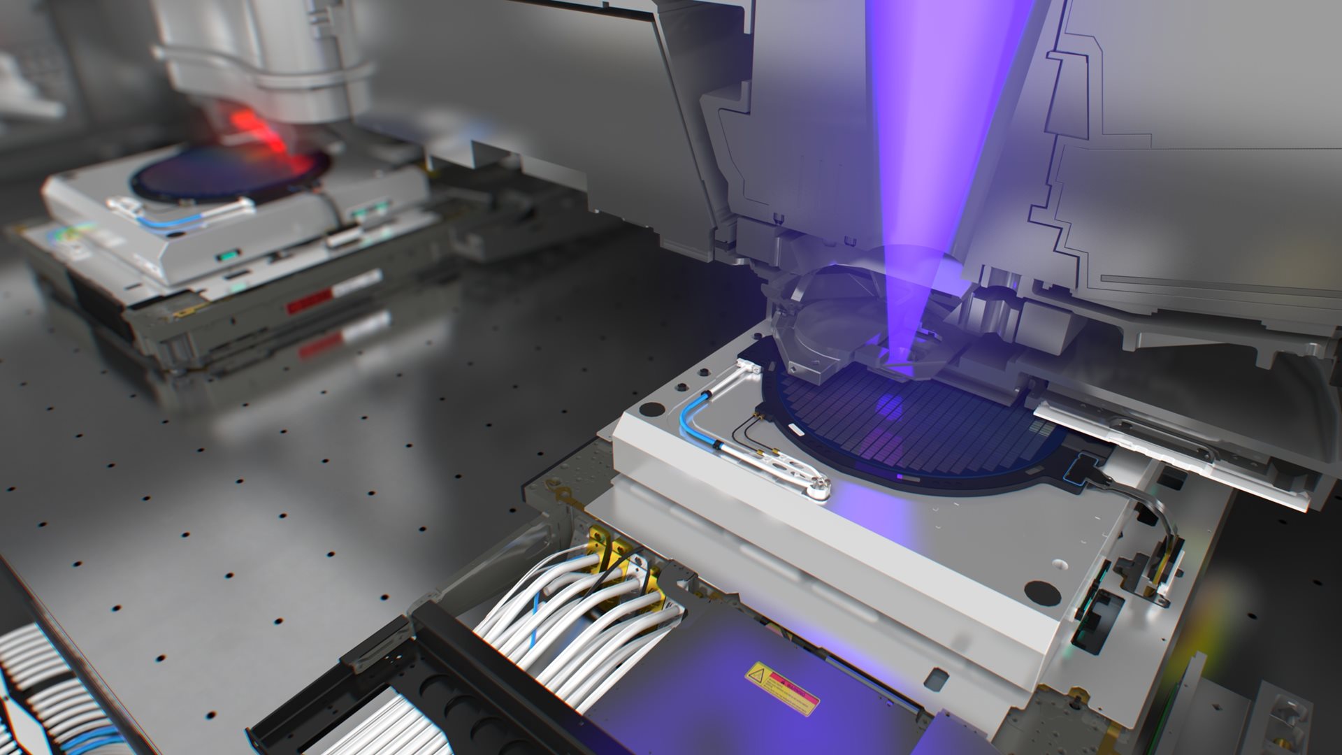
Developed for volume production applications, the 300 mm TWINSCAN AT:1100 is a 193 nm wavelength system with the industry's highest numerical aperture ArF lens. ASML has been the leading supplier of high numerical aperture 193 nm solutions to the industry since June 2001 through its 200 mm PAS 5500 Step & Scan platform. TWINSCAN features dual wafer stage technology that enables the exposure of one wafer and the alignment of the next wafer to take place in parallel, giving higher throughput and increased productivity.
About ASML


