Press release - Veldhoven, the Netherlands, August 9, 2001
ASML today announced it has shipped the first of its new PAS 5500/800 KrF Step & Scan lithography systems, which offer the industry's highest numerical aperture (NA) of 0.80, to leading-edge DRAM memory manufacturers. The systems, with resolution specified for 120 nm, will be used for volume production of 256 MB DRAMs and other advanced memory devices such as Flash and very fast SRAMs.
"The PAS 5500/800 will enable these leading-edge manufacturers to extend their investment in mature KrF technology to new generations of memory products," said Dave Chavoustie, executive vice president of sales for ASML. "By demonstrating our ability to extend the PAS 5500 platform and provide new tools, our systems continue to deliver very high productivity and low cost of ownership."
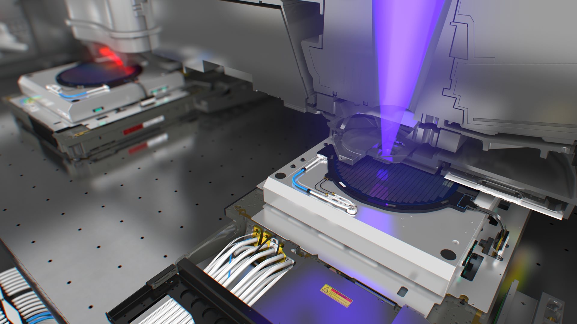
Announced in January 2001, the PAS 5500/800 has a throughput specification of 115 200 mm wafers per hour. The system is designed for high-volume processing of today's most advanced ICs, as well as R&D and pilot production for next-generation logic, ASIC and advanced memory devices. The PAS 5500/800 combines the imaging power of Carl Zeiss StarLith 800 0.8 NA, 4X reduction lens with AERIAL II illumination technology to optimize process latitude across the range of critical dimensions and circuit design features. The system is equipped with ASML's patented ATHENA wafer alignment system and the newly developed reticle blue alignment allowing actinic wavelength reticle alignment, enabling single machine overlay accuracy of less than 20 nm. A new level sensor improves focus accuracy to enhance process control and yield, particularly for edge dies. Customers can choose from the three leading suppliers of 20-watt KrF lasers. ASML's implementation for the laser source includes variable laser frequency control, which combined with high optical transmission through the illumination and projections optics ensures higher productivity and lower operating costs.
About ASML


