Press release - Veldhoven, the Netherlands, September 16, 2001
ASML today announced the shipment of the first production unit of its new dual wafer stage TWINSCAN 300 mm lithography system to Taiwan Semiconductor Manufacturing Company Ltd. (TSMC), the world's largest dedicated semiconductor foundry.
TSMC will install the TWINSCAN AT:750 system at its 300 mm Fab 12 in Hsinchu, Taiwan. TSMC is already using the TWINSCAN platform in production, having taken delivery of the first single stage version, TWINSCAN AT:700S, last year.
"The silicon foundry business demands flexible, high-productivity tools that can accommodate small batches and quick turn-times," said Dr. Nun-Sian Tsai, senior director of the 300 mm pilot line project at TSMC. "We have been pleased with the superior imaging and overlay performance of the AT:700S single wafer stage tool that we installed last year. The AT:750 combines this performance ability with the productivity advantages associated with the dual wafer stages."
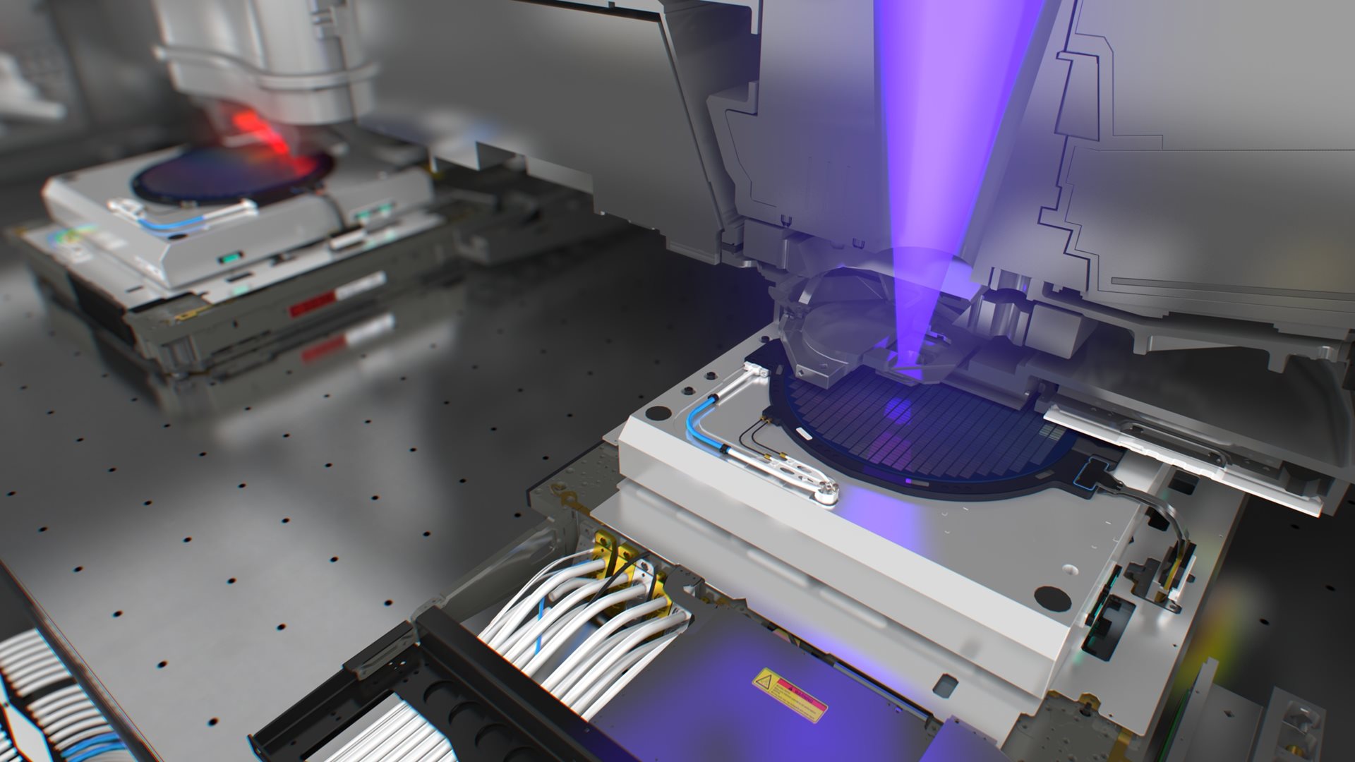
TSMC selected the high-productivity imaging system based on the inherent advantages offered by ASML's unique dual stage architecture. While the wafer on one stage is being exposed, the wafer on the second stage can be aligned and have its surface mapped by an interferometer, virtually eliminating non-productive overhead time. The separation of the alignment and exposure operations allows more extensive and accurate alignment and wafer surface height mapping of the entire 300 mm wafer without impacting throughput. It is this increase in metrology accuracy that is essential for delivering the critical dimension control and overlay across the wafer at full throughput.
"Foundry customers need a lithography solution that provides the productivity needed for them to generate return on investment and the flexibility to work across multiple product types," said Don Crabtree, ASML vice president of sales for Asia. "TSMC's decision to go with the dual-stage TWINSCAN platform shows that the architecture satisfies TSMC's needs on both counts."
The TWINSCAN product family includes four systems, enabling chipmakers to implement cost-effective mix-and-match strategies for the lowest production costs. Designed for 300 mm wafers, the TWINSCAN product family is composed of three dual wafer stage systems the AT:1100 , the AT:750 and the AT:400 and the single wafer stage AT: 700S . The platform ranges from 365 nm to 157 nm wavelength.
About ASML
About TSMC


