Press release - Veldhoven, the Netherlands, April 22, 2002
ASML today announced that the company has received the industry's first order for an extreme ultraviolet (EUV) lithography beta tool from Intel Corp., the world's largest semiconductor manufacturer. The EUV beta tool will use 300 mm wafers and is initially targeted for 45 nm resolution capability. Delivery is slated for the second half of 2005.
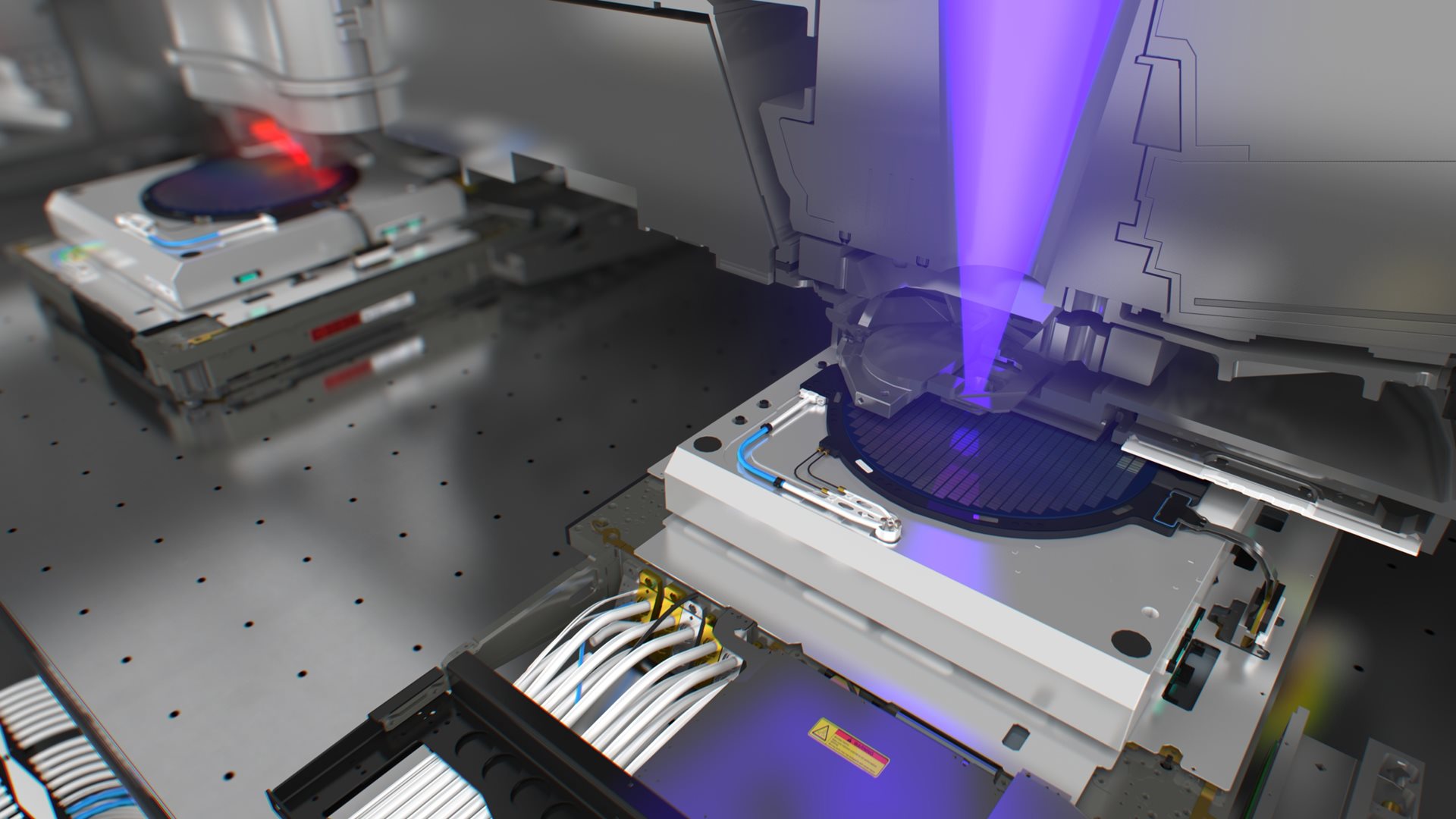
EUV lithography is an extension of optical lithography techniques into extreme ultraviolet wavelengths. EUV uses light with a wavelength of 13.5 nm (more than 10 times shorter than current lithography technology) to image critical layers with feature sizes below 45 nm. The new technology also differs from existing optical lithography in that it uses reflective optics and reflective reticles (photomasks).
"The sale of the first EUV beta tool is much more than the sale of a new tool to a customer. It represents the culmination of many years of work on the selection, development and engineering of next generation lithography technologies," said Martin van den Brink, ASML executive vice president of marketing and technology. "Intel has confirmed its commitment to EUV and ASML's EUV capability."
Since 1999, ASML has been a supplier to and licensee of the EUV Limited Liability Company, an organization of semiconductor manufacturers, including Intel, dedicated to developing this technology. ASML continues to work closely with all of the member companies to develop and refine every aspect of EUV, including the necessary photomasks and photoresists to make the technology commercially viable and ready for production.
ASML's EUV tool will incorporate a dual-stage architecture that is similar to the company's TWINSCAN platform and will have the capability to meet industry productivity and cost of ownership targets. However, the shorter wavelength of light used in this technology demands that the entire optical path as well as the reticle and wafers stages be housed in a vacuum environment, requiring entirely new engineering and subsystems modules.
"This new technology requires revolutionary innovation from our technology partners as well as our US and European development teams, which are based in Wilton, Connecticut, and Veldhoven, the Netherlands," van den Brink said. "The challenges are significant, but we are confident in our ability and commitment to meet the industry need for this advanced EUV next-generation lithography."
About ASML


