Press release - Veldhoven, the Netherlands, November 12, 2003
ASML Holding NV (ASML) in a meeting tomorrow with investors and financial analysts will highlight several of the company’s operational and technological developments.
ASML will review its updated technology roadmap in response to future imaging challenges as the demand for ‘shrink’ (smaller features) continues. Capabilities and customer benefits of ASML’s recently launched TWINSCAN XT:1250 system will be detailed. Europe’s largest independent R&D center IMEC will present a synopsis of its 157 nm project, conducted on the ASML Micrascan VII. Maskless lithography technology will be explained and the market opportunity explored. From a business infrastructure perspective, ASML will review accomplishments from cost-cutting measures in operations and suppliers’ improvements in cost and flexibility.
Positive immersion program results
The ASML Analyst Day agenda includes a presentation on the early successes achieved by the company in its immersion lithography program. The market for immersion lithography tools is projected to go from zero to US$ 230 million by 2005, according to industry analysts.
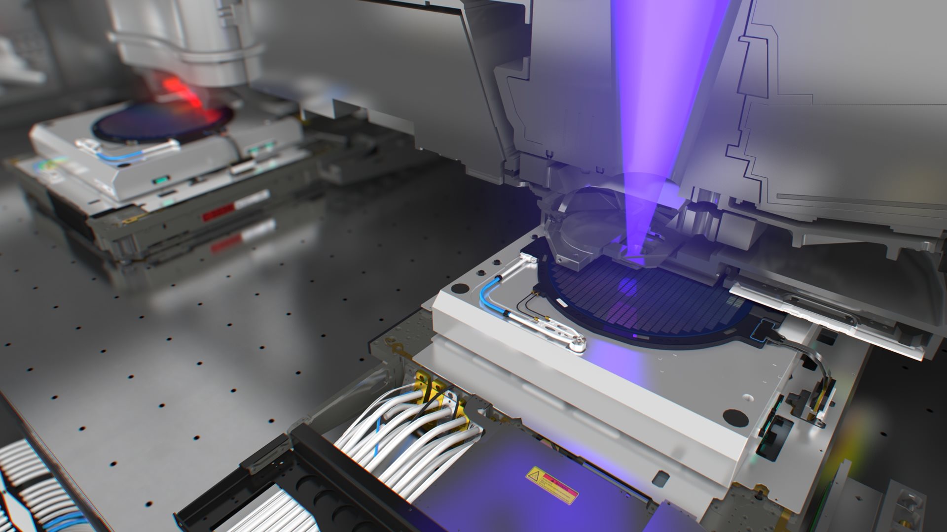
Immersion lithography replaces the air between the wafer and the lens with fluid to improve depth of focus and extend wavelengths to lower nodes. ASML began exploring this technology in the first half of 2002 and, in early 2003, began testing immersion processes on its TWINSCAN lithography systems. Initial, positive results from the program include:
- ASML has a unique competitive advantage in immersion due to the dual-stage design of its TWINSCAN system. The immersion fluid needed for imaging can be applied between the wafer and the lens at one stage (the exposure station) while the measuring of the wafer – focus and overlay – is completed in the other, dry stage (the metrology station). Customers continue to measure in air rather than incurring the costs of new calibration processes needed for ‘wet’ metrology.
- ASML’s existing lens designs can be easily adapted to immersion without an optical redesign.
- Through immersion, ASML can extend the life of the current 193 nm node. This allows customers to continue to benefit from existing technology investments.
- ASML can apply immersion processes to 157 nm technology as a solution reaching below the 45 nm node.
All presentations from ASML Analyst Day will be available on the company’s website at www.asml.com on Thursday, November 13, 2003.
About ASML


