Press release - Veldhoven, the Netherlands, October 21, 2003
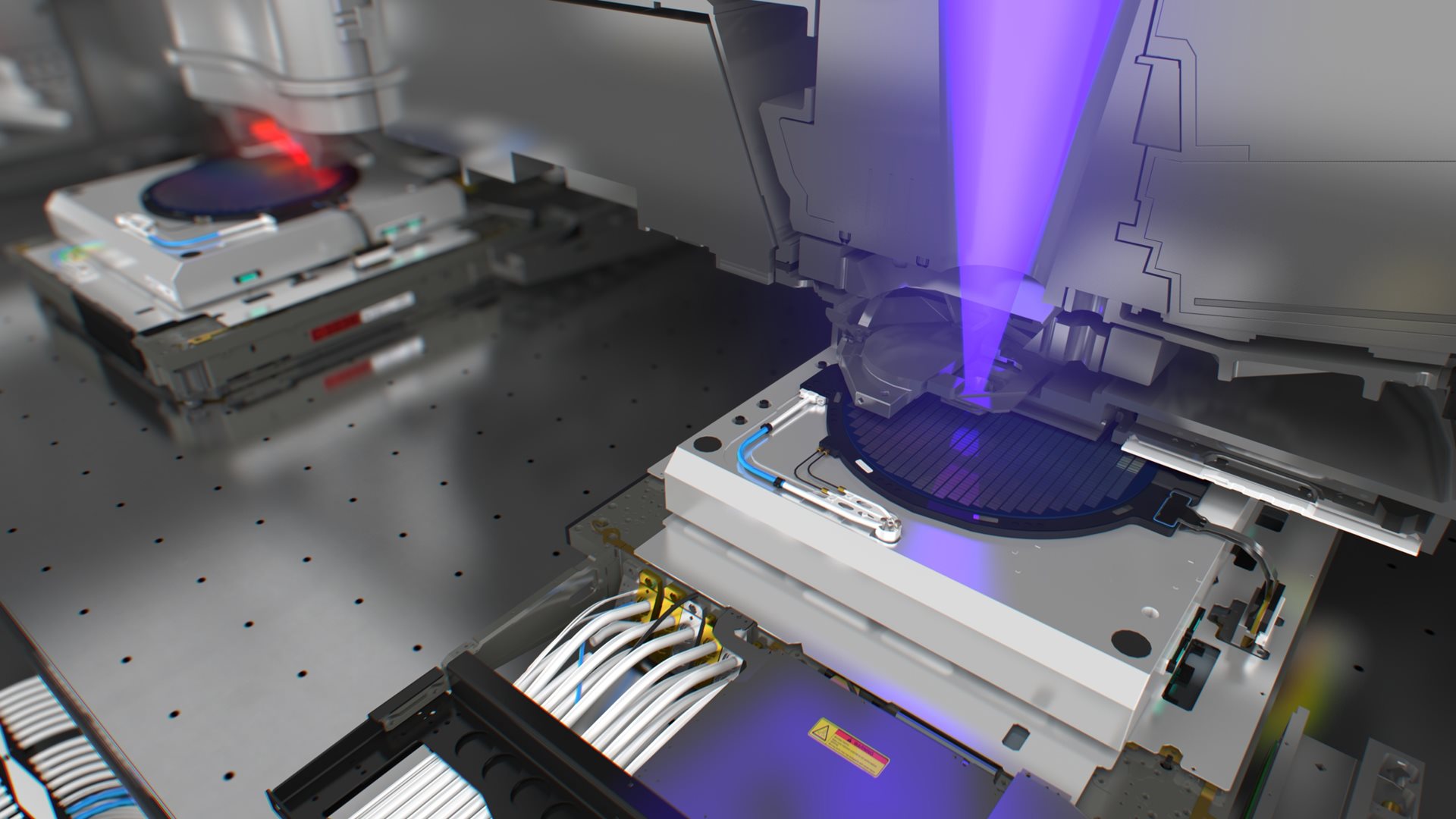
ASML Holding NV (ASML) today introduced the new generation of its TWINSCAN platform – TWINSCAN XT:1250 – a 0.85 NA, 193 nm volume production lithography scanner that extends imaging to the 65 nm node on both 200 mm and 300 mm wafers. ASML has already booked several customer orders for the XT:1250 with initial deliveries scheduled for the second quarter of 2004.
“ASML’s commitment to customers drives the functionality and design of the TWINSCAN XT:1250. After conducting a global survey, we concluded that chipmakers wanted a tool that cost-effectively manufactures smaller, faster chips and maximizes customer investment in existing 193 nm infrastructure,” said Doug Dunn, president and CEO, ASML. “TWINSCAN XT:1250 achieves this through its extendibility to the 65 nm node, its availability in either 200 mm or 300 mm models, and its modular design.”
The greatest challenges in manufacturing faster chips is printing the incredibly small – sub-micron – circuit features in precise alignment – measured in nanometers – with as many as two-dozen separate layers. The XT:1250 patterns those minute features accurately, based on the stability and reliability of the proven TWINSCAN platform.
The XT:1250 features Ultra-k1, a hardware and software portfolio that extends the capabilities of 193 systems. This package of proprietary products gives chipmakers the ability to continue to shrink circuit features, ensures high die yields and maximizes bottom-line return. The Ultra-k1 portfolio dramatically improves process latitude, depth of focus and critical dimension (CD) control.
To provide chipmakers with highest value of ownership, ASML reduced the XT:1250 footprint by 25%. This was achieved by placing components from the original system into redesigned, compact support modules that can be located in the sub-fab. Additionally, all TWINSCAN systems benefit from a 50% reduction in specified installation facility requirements, such as power consumption, process cooling water, clean dry air and exhaust flow.
About ASML


