Press release - VELDHOVEN, the Netherlands, May 20, 2003
ASML Holding NV (ASML) today announced the sale of an advanced lithography system to Singapore-based UMCi, a 300 mm foundry joint venture company between UMC, Infineon Technologies and Singapore’s Economic Development Board Investments (EDBI). At full capacity, UMCi’s wafer foundry will produce up to 40,000 wafers per month.
“UMCi continues to install the world’s most advanced manufacturing systems in our Singapore fab as we proceed with the facility’s equipment move-in. The ASML TWINSCAN platform offers outstanding performance in a demanding, real-world environment. The tool’s high productivity and excellent imaging quality will be a valuable asset as we move to production later this year,” said Chris Chi, president, UMCi.
Over the last few years, semiconductor companies have begun to shift from 200 mm wafers to 300 mm wafers, as the larger size can increase yields and lower production costs. Semiconductor Equipment and Materials International (SEMI) estimates that by 2006, there will be eleven 300 mm fabs in the world. When fully functioning, these eleven fabs will produce 282,000 wafers per month.
“ASML secured an early lead in selling advanced lithography systems to the dedicated foundries of the world operating 300 mm fabs. We are committed to providing technology that adds value to customers in industries with high quality standards and no room for error,” said Doug Dunn, president and CEO, ASML.
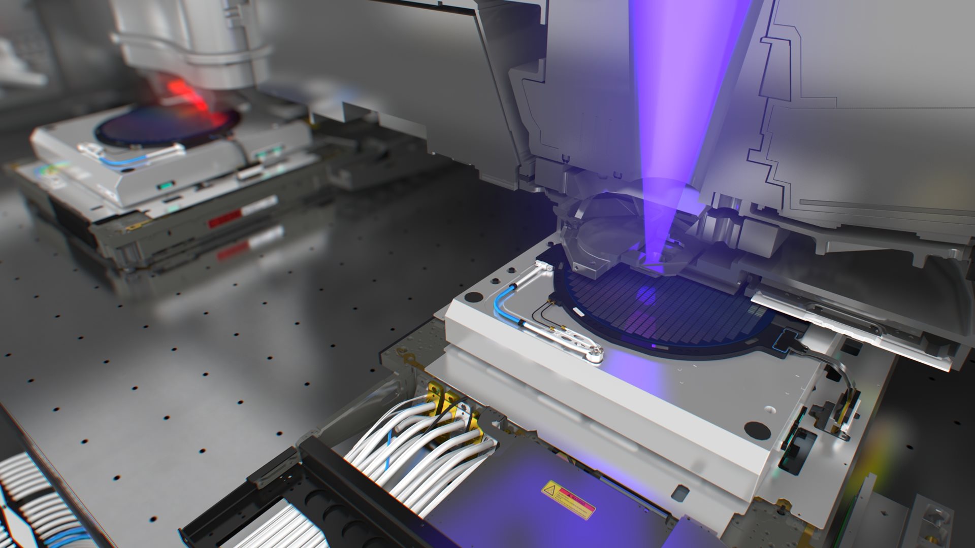
UMCi will use ASML’s AT:850B lithography system to image 0.13-micron circuits on 300 mm silicon wafers for the production of advanced chips. The AT:850B platform is a member of ASML’s TWINSCAN family of optical lithography systems for 300 mm production down to the 80-nanometer technology node.
About ASML


