Press release - Santa Clara, California, December 1, 2004
Applied Materials, Inc. and ASML today announced a unique collaboration intended to speed the development of 65 nm and below process equipment technology for the semiconductor industry. As part of this agreement, ASML will deliver one of the world’s first immersion lithography systems, its TWINSCAN XT:1250i step-and-scan system, to Applied’s Maydan Technology Center (MTC) in early 2005. The step-and-scan system will be used in conjunction with Applied’s broad range of systems at the MTC to develop integration-worthy process tools, demonstrate the manufacturing-readiness of equipment, and optimize processes for minimal defects.
“Having ASML’s latest immersion lithography capability at our MTC demonstration facility will provide Applied the same leading-edge scanning technology used by our most advanced customers as they enter 65 nm and beyond production,” said John T.C. Lee, general manager of Applied Materials’ Maydan Technology Center group. “Our collaboration with ASML will generate new information about key lithography and process issues facing the equipment industry. This is expected to dramatically enhance both companies’ ability to develop highly advanced process flows, leading to best-of-breed products for next-generation manufacturing to meet our customers’ most critical requirements.”
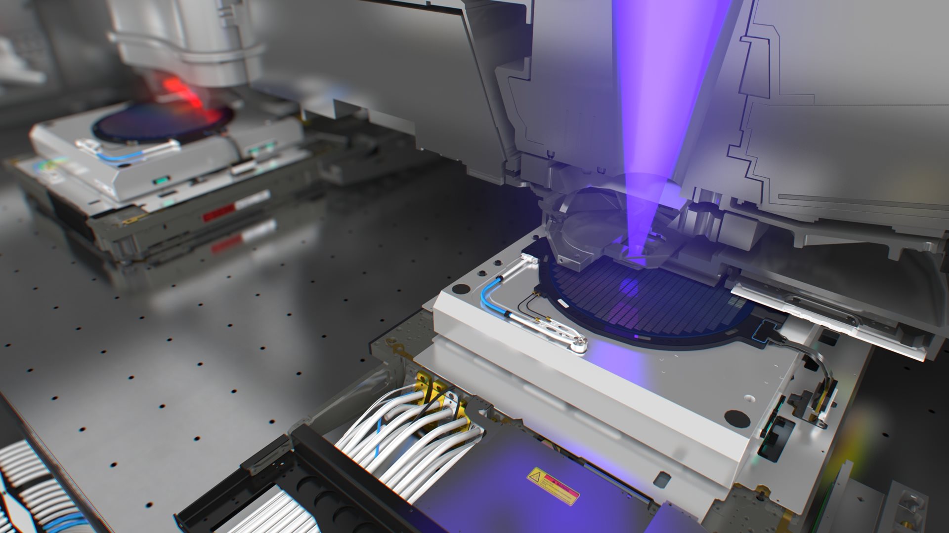
Immersion lithography differs from conventional 'dry' lithography in that the air between the wafer and the lens is replaced with water to improve depth of focus and extend wavelengths to lower nodes. Immersion lithography uses hyper-NA lenses, allowing the patterning of smaller linewidths without having to develop an expensive new light source, and enabling the extension of 193nm lithography to the 45nm node. ASML’s TWINSCAN XT:1250i system is a 300 mm wafer, dual-stage design that combines the improved depth of focus of immersion tools with the minimum resolution of dry lithography systems.
Dave Chavoustie, executive vice president, sales, ASML, said, “The relationship between lithography and process technology has become extremely critical at the 65 nm generation. We chose to collaborate with Applied Materials because of its broad portfolio of equipment for both front- and back-end wafer processing. This agreement will provide ASML with an opportunity to qualify our immersion lithography technology with a set of leading-edge process tools and provide customers with critical electrical and yield data from process equipment interactions with immersion lithography. Having our latest step-and-scan system at the MTC will also give customers greater access to our system and encourage new collaborative efforts.”
The ASML-Applied Materials team will also take advantage of Applied’s process diagnostic and inspection tools in the MTC to speed defect learning of the immersion lithography process. Defects that may arise as a result of working with several new materials can be quickly reviewed and identified, helping to enable the acceleration of customers’ 65 nm and below process development.
About ASML
About Applied Materials


