Press release - Veldhoven, the Netherlands, April 20, 2004
ASML Holding NV (ASML) today introduced the newest member of its TWINSCAN platform, the TWINSCAN XT:1400. The system is a 0.93 NA, 193 nm scanner that images at the 65 nm node in volume production environments. The XT:1400 can also be used for pre-production testing and development at the 45 nm node. The first shipments are slated for December 2004.
The XT:1400 has a unique architecture found only in ASML systems. The design provides customers with the option of transitioning the system from 'dry' to immersion lithography on the fab or factory floor through an ‘immersion conversion’ kit available in Q4 2005. The XT:1400 gives customers the flexibility to include immersion into their technology roadmaps while protecting their investments in dry 193 nm technology.
"ASML innovations focus on evolving customer needs. The XT:1400 is packed with choices. Customers can either volume-produce chips at the 65 nm node or develop their processes for chip manufacturing at the 45 nm node," said Martin van den Brink, executive vice president, marketing and technology, ASML.
"The strategy behind our high NA, immersion-prepared system means chipmakers move towards new technologies at their own pace and with minimum investment. This significantly lowers the risk traditionally associated with wavelength reductions. The XT:1400 constitutes ASML’s third generation of immersion tools – the 1150i was our prototype and the XT:1250i was our pre-production tool, both were announced last year," van den Brink concluded.
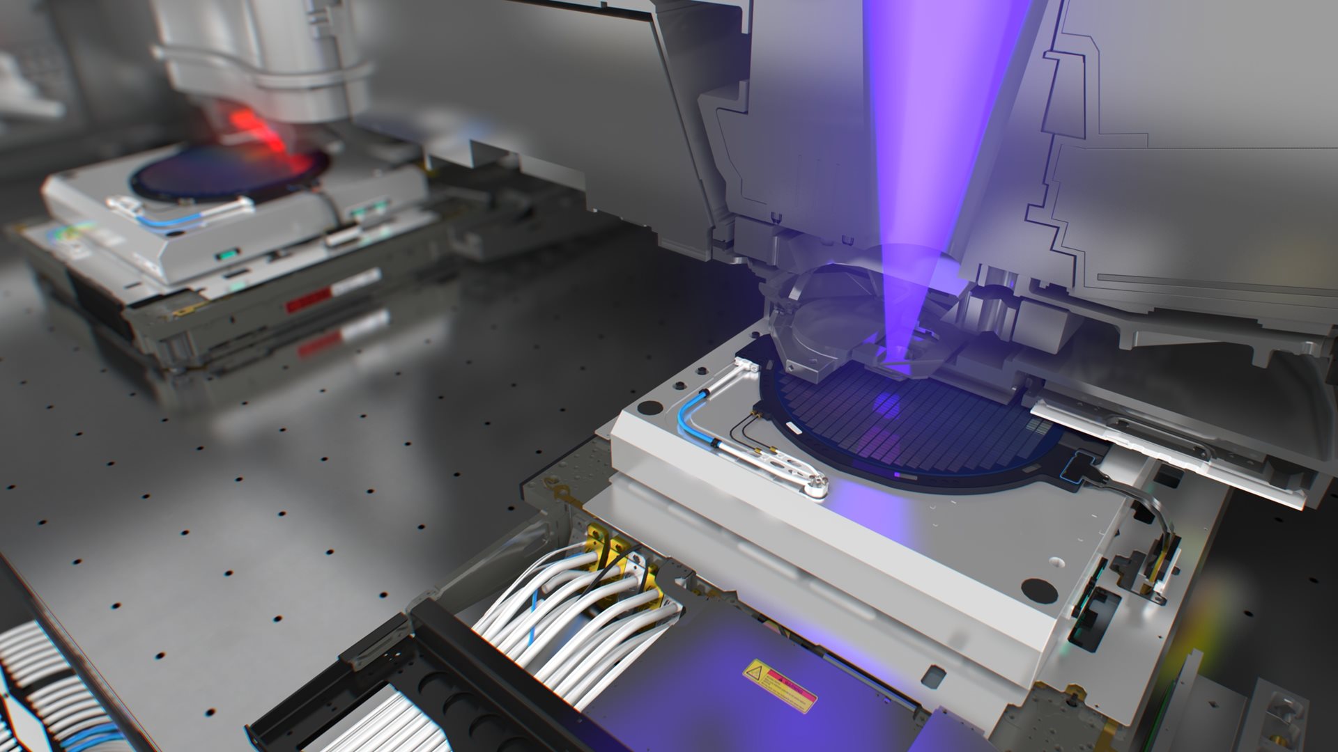
The immersion conversion kit for the XT:1400 is comprised of three main components – a lens suitable for immersion use, immersion-compatible wafer stages and immersion infrastructure. Conversion from a dry to a wet platform can be achieved in a matter of weeks and will increase the process latitude of the system.
The XT:1400 comes equipped with Ultra-k1, ASML’s hardware and software portfolio of imaging enhancement technologies that allows the shrinking of circuit features, ensures high die yields and maximizes bottom-line return.
About ASML


