Press release - SEMICON JAPAN, Tokyo, Japan, December 7, 2005
ASML Holding NV (ASML) today announced significant progress towards development of both high-NA immersion and extreme ultraviolet (EUV) lithography technology: two critical elements of the semiconductor industry’s ability to continue its historical trend of packing more power onto silicon chips.
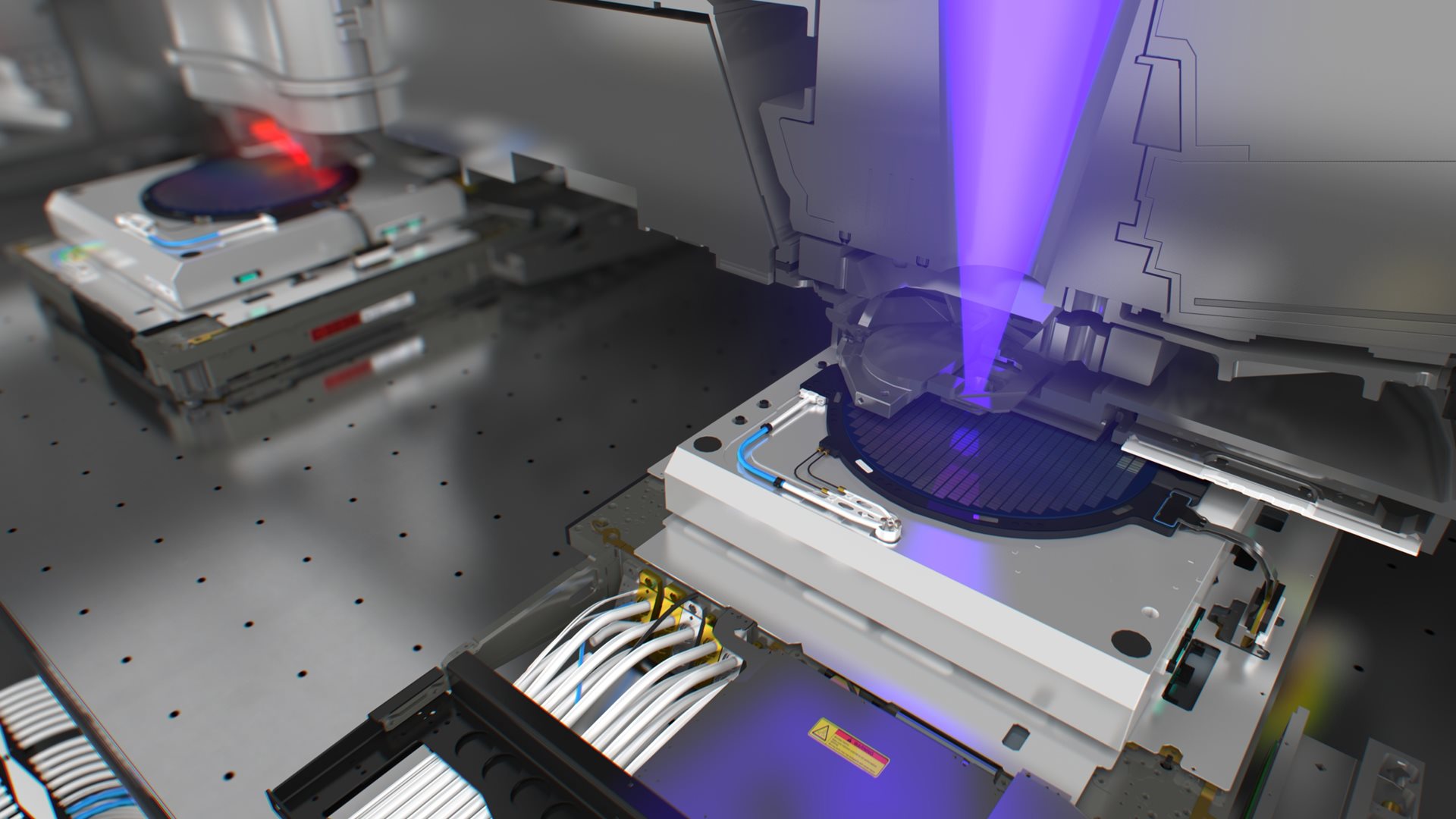
ASML presented the first resist images produced by its TWINSCAN XT:1700i. These breakthrough results are made possible by the combination of a 1.2 numerical aperture (NA) catadioptric lens, polarized illumination and water-based immersion technology. The lens is performing well within specification and is now ramping up for production. Qualification of the total system is ongoing and the first tool will be ready for shipment by the end of Q1 2006. ASML has multiple orders for this fourth-generation immersion tool and expects to ship between 20 and 25 immersion systems in 2006, including shipments to Japan.
In addition, ASML marks significant progress on its EUV alpha tool development: collaborating vendors of mask blanks (SCHOTT Lithotec), photomasks (Toppan Photomasks) and optical systems (Carl Zeiss SMT) have been shipping their respective components to ASML. While the assembly of two alpha tools is in progress, the first projection system is being qualified and integrated, an important proof-of-concept for EUV lithography. ASML plans to ship the world’s first 0.25 NA EUV alpha tools in Q2 2006 to the Interuniversity MicroElectronics Center (IMEC) in Leuven, Belgium, and Albany NanoTech at the State University of New York at Albany, New York.
“The progress achieved in high NA immersion and EUV is compelling because both technologies offer real options for 32 nm lithography and beyond. Also, double exposure/double patterning should be considered to possibly extend 193 nm lithography,” said Martin van den Brink, ASML’s executive vice president, Marketing and Technology. “The industry must make roadmap choices and ASML is committed to align to the roadmap of its key customers. As always, we will provide access to early tools for collaborators, vendors and customers. Hands-on experience fosters industry-wide collaboration and will clarify roadmap choices.”
About ASML


