Press release - San Jose, California, February 22, 2006
ASML Holding NV (ASML) today presented its latest advances in leading-edge production technology as well as its research and development (R&D) progress at SPIE Microlithography 2006 in San Jose, California. Images down to 42 nanometers printed on the ASML TWINSCAN XT:1700i system were shown along with results that support the viability of this tool for volume production across several nodes. In addition, ASML presented proof-of-concept 35 nm images from its extreme ultraviolet (EUV) Alpha-Demo Tool (ADT), which is rapidly progressing in imaging qualification.
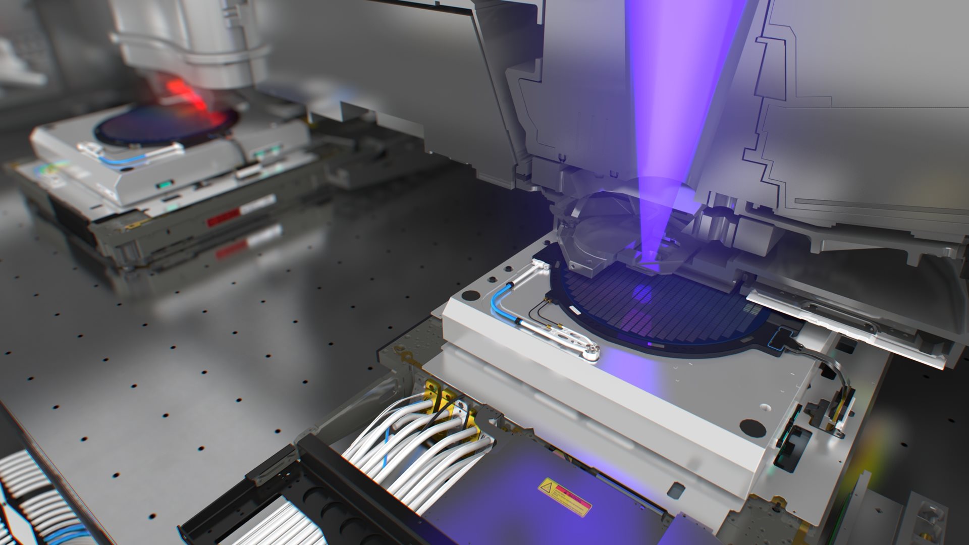
The XT:1700i, ASML’s fourth-generation immersion system, features a 1.2 numerical aperture (NA) catadioptric lens and provides a 30% improvement in resolution compared with today’s leading-edge dry tools. ASML’s presentations demonstrate that the XT:1700i supports volume production at 45 nm.
ASML disclosed TWINSCAN XT:1700i images of record resolution of 42 nm dense lines at a 84 nm pitch with a depth of focus of 1 micron at a field size of 26 mm x 33 mm. ASML also reported significant progress in defectivity levels of its immersion technology, demonstrating that champion data are meeting production requirements.
ASML expects to ramp up volume production of XT:1700i systems in Q2 2006, enabling the semiconductor industry’s transition to 45 nm imaging. To date, ASML has delivered 13 immersion systems based on the company’s XT:1150, XT:1250 and XT:1400 ArF lithography technology. These systems continue to enable mature immersion processing capability.
ASML disclosed that it received its first customer request for a system conversion in the field from dry to wet. The company has already shipped more than 50 systems which can be converted into an immersion tool. More conversions are expected as customers consider to take advantage of increased depth of focus latitude for 65 nm applications now that immersion processes are becoming mature enough for production deployment.
ASML also presented new results from its EUV ADT imaging qualification stage, including proof-of-concept 35 nm images which could be obtained over the full slit of 26 mm. The first of two EUV alpha demo systems is fully assembled: its metrology sensors, wafer and reticle stages, and material handling modules are qualified, and the complete optical train (including illuminator and projection optics) is now in the final qualification process.
ASML expects its EUV systems will be a critical enabler not only for EUV infrastructure development for 32 nm lithography but also for the commercialization of EUV lithography. ASML plans to ship the world’s first 0.25 NA EUV systems in Q2 2006 to Albany NanoTech at the State University of New York at Albany, NY, and the Interuniversity MicroElectronics Center (IMEC) in Leuven, Belgium.
About ASML


