Press release - San Francisco, California – SEMICON West, July 16, 2007
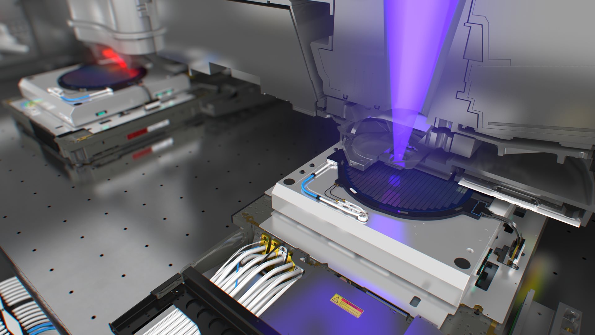
ASML Holding NV (ASML) today announced a new KrF lithography system that significantly reduces operating costs for its customers. The ASML TWINSCAN XT:1000 scanner extends cost-efficient KrF technology to resolutions that previously required more expensive ArF technology. Customers can realize savings of 30% or more per layer as a result of lower operating costs for KrF technology, particularly from cheaper lasers and lower materials cost such as KrF resists.
Today KrF systems account for about 35% of the total semiconductor lithography market (units). By introducing the XT:1000, ASML shows its commitment to cost-effective production systems. The XT:1000 provides benefits for both logic and memory manufacturers.
The XT:1000’s high numerical aperture (NA) of 0.93 can resolve 80-nanometer (nm) device features, far smaller than the 100 nm of today’s KrF systems. The XT:1000 also improves value for customers, with an increased throughput of 165 300 mm wafers per hour under volume manufacturing conditions while maintaining the same industry-leading 6 nm overlay as leading edge ArF systems.
“ASML understands that lithography needs to be cost-effective as well as technologically advanced,” said Martin van den Brink, executive vice president of marketing and technology at ASML. “Our goal is to reduce our customers’ cost per wafer. The XT:1000 allows them to produce chips with less costly KrF tools, even as they shrink their devices.”
ASML expects to begin shipping the XT:1000 by mid-2008.
About ASML
About KrF and ArF technologies


