Press release - San Jose, California, February 26, 2007
ASML Holding NV (ASML) today announced that it will present record imaging results for immersion and extreme ultraviolet (EUV) technologies during SPIE Microlithography 2007. ASML will show two sets of breakthrough lithography results at the annual conference, including 37 nm dense lines produced on the TWINSCAN XT:1900i, and both 32 nm dense lines and 32 nm dense contact holes from ASML full-field EUV Alpha Demo Tools (ADT).
"Our customers require new technologies to get them beyond the 45 nm node," said Martin van den Brink, executive vice president of marketing and technology at ASML. "The industry's first full-field EUV results from a customer site, coupled with the best resolution achieved to date for immersion, demonstrate how our technologies continue to support our customers and their respective roadmaps."
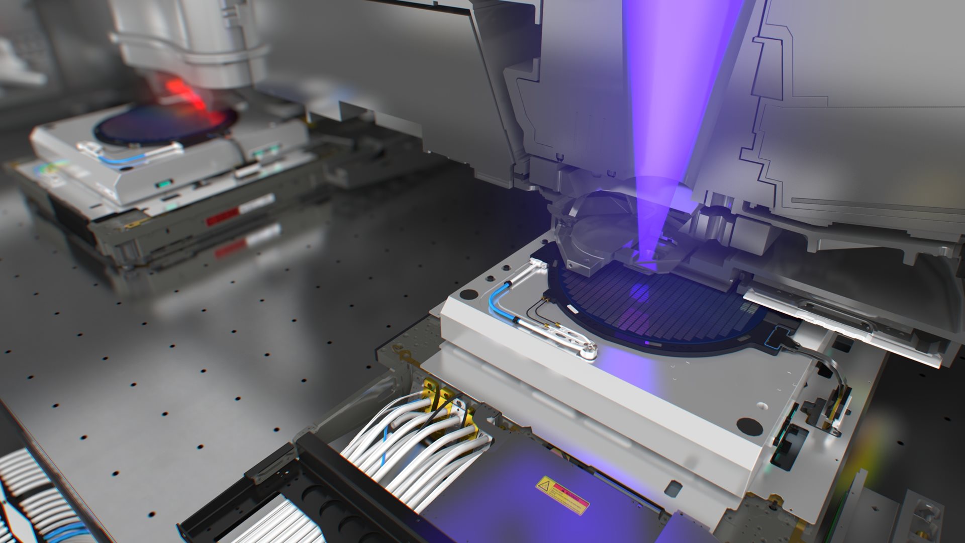
The industry adoption of immersion lithography and ASML's leadership in advanced exposure technologies is proven by more than 36 immersion systems shipped by ASML. ASML’s TWINSCAN XT:1700i immersion scanner is now ramping up for production at customer sites. ASML's 37 nm results were accomplished on the TWINSCAN XT:1900i. This next-generation immersion system features the same advanced catadioptric lens design as the XT:1700i, but with better resolution capability due to the higher numerical aperture of 1.35. The throughput has increased to 131 wafers per hour.
In addition to the immersion results, ASML will also present 32 nm dense lines and 32 nm dense contact holes using EUV lithography. This technology still promises to give the most cost-effective and extendible option for production at the 32 nm node and beyond. ASML was the first to ship full-field EUV systems to customers, and currently has orders for three EUV pre-production systems. The first shipments are planned for 2009.
About ASML


