Press release - Veldhoven, the Netherlands, July 18, 2007
ASML Holding NV (ASML) today announced that it has shipped its first TWINSCAN XT:1900i, the world’s only lithography system capable of imaging features down to 36.5 nanometers (nm) on chips manufactured in volume. Production of the XT:1900i is now ramping up fast, as multiple orders have been placed and systems will be shipped before the end of this year to many of the world’s leading device makers.
These customer orders demonstrate that leading memory and logic makers are selecting the XT:1900i to help them accomplish their strategic technology goals. Chipmakers need to produce ever smaller and denser integrated circuits to improve the functionality of their chip designs to power today’s computing and consumer electronics products.
“ASML’s immersion technology meets the demanding requirements of the world’s top IC makers, said Martin van den Brink, executive vice president of marketing and technology at ASML. “The XT:1900i, the latest addition to our production-proven line of immersion tools, allows customers to extend their high-volume manufacturing capabilities to an unprecedented 36.5 nm resolution.”
The implementation of immersion technology in production is making fast progress resulting in the fact that to date, more than two million wafers have been processed on ASML’s TWINSCAN immersion systems in total and half of that in the last quarter.
About the TWINSCAN XT:1900i
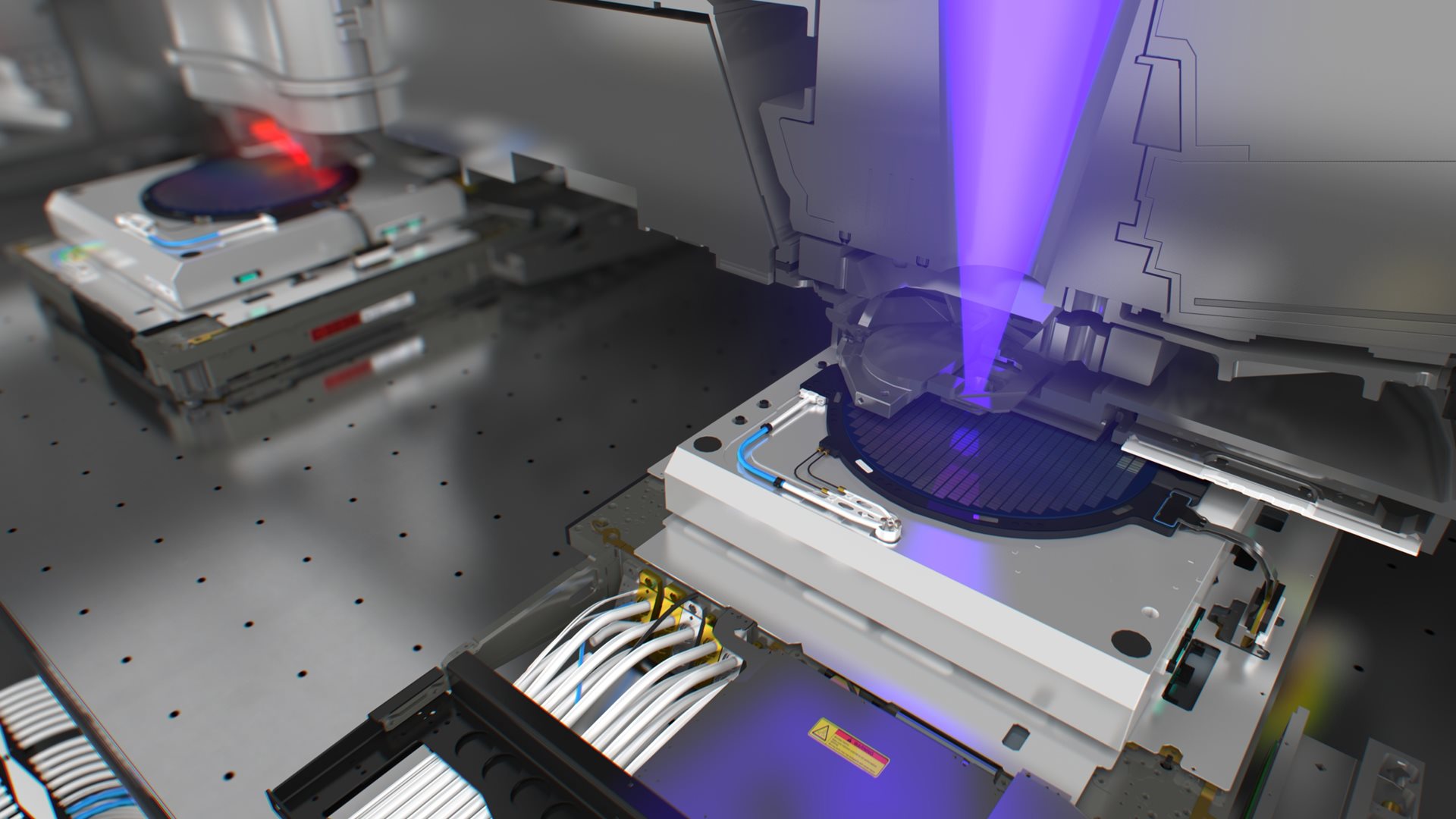
The TWINSCAN XT:1900i with HydroLith immersion technology places liquid between the lens and the silicon wafer, enabling chipmakers to produce smaller features while using a light source with the same wavelength. Immersion technology also improves the depth of focus or quality of the image to be drawn on a chip compared to dry imaging at similar resolution. The XT:1900i builds on the proven performance of the XT:1700i, which is currently used in volume production. The XT:1900i offers the highest numerical aperture available (1.35) and has demonstrated industry-leading performance of 36.5 nm resolution, 4.6 nm single-machine overlay and 131 wafers-per-hour productivity.
About ASML


