Press release - TOKYO, SEMICON Japan, December 5, 2007
ASML Holding NV (ASML) today announces rapid industry adoption of the TWINSCAN XT:1900i, which began shipping in July 2007. The XT:1900i enables volume production of logic devices down to 32 nanometers (nm) and memory devices at 40 nm. Chipmakers need to produce ever smaller and denser integrated circuits to improve the functionality of their chip designs to power today’s computing and consumer electronics products.
“The move to immersion technology is one of the fastest technology transitions in the history of the industry,” said Martin van den Brink, executive vice president of marketing and technology at ASML. “And the adoption of the XT:1900i has led to one of the quickest-ever product ramps for ASML.”
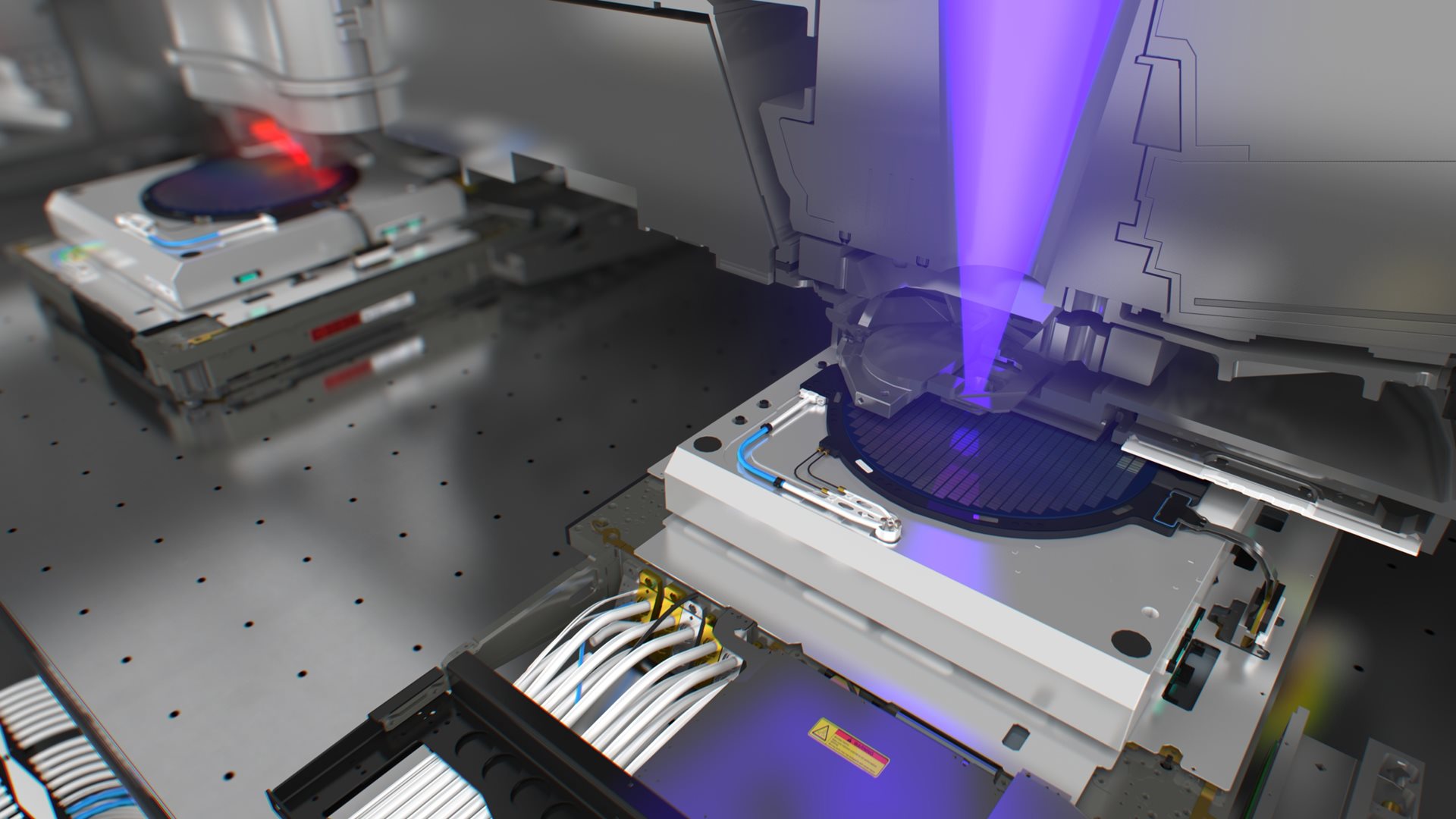
The XT:1900i is ASML’s latest immersion lithography system and the semiconductor industry’s most advanced. The XT:1900i offers the highest numerical aperture (NA) in the industry today (1.35), enabling the finest possible production resolution. ASML expects to ship 15 to 20 XT:1900i systems this year, including several to Japanese chipmakers.
ASML immersion systems have imaged more than six million wafers to date. By the end of 2007, ASML will have shipped more than 70 immersion systems to 20 different customers on three continents.
“ASML’s immersion technology is helping Japanese customers meet their roadmap requirements,” said Hiroshi Ishiwata, president and representative director, ASML Japan. “Japan’s leading memory chipmakers are adopting the TWINSCAN platform to produce their leading-edge devices because of its productivity, overlay and imaging performance.”
ASML’s installed base of TWINSCAN XT:1700i and XT:1900i immersion systems has been growing rapidly in Japan, including three customers who have taken delivery of multiple systems. One-third of ASML’s 12 immersion systems shipped during this year’s third quarter went to Japanese customers. To support its growing business, ASML is increasing its Japanese workforce to more than 200 employees, of which about 80% are engineers. Over 70% of ASML’s products go to customers in Japan and the Asia-Pacific region.
About ASML
About immersion technology


