Press release - Tokyo, Japan, December 3, 2008
ASML Holding NV (ASML) today announces at SEMICON Japan the first system based on its new TWINSCAN NXT lithography platform. The TWINSCAN NXT:1950i provides the increased productivity and extremely tight overlay that will enable chip manufacturers to shrink feature sizes to 32 nanometers and beyond in order to reduce costs – a nanometer is a millionth of a millimeter.
Feature shrink is the primary semiconductor cost reducer and chipmakers continue to shrink their designs as aggressively as they can. Today, this shrink is enabled by single-exposure immersion lithography. Double-patterning techniques with immersion scanners will also be used to make chip features smaller and continue Moore’s Law – which states that the number of transistors on a chip doubles every 24 months.
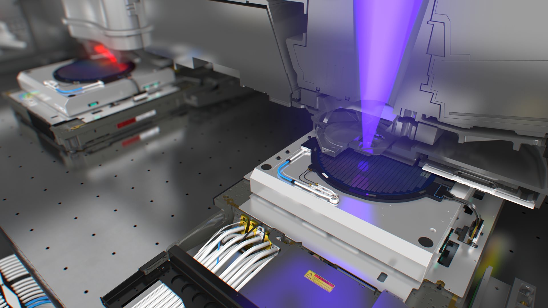
Double-patterning poses productivity challenges for chipmakers because a chip’s critical layers need to be exposed and processed twice, adding complexity and cost. At the same time, chipmakers demand ever more efficient single-patterning processes to remain competitive. ASML addresses these challenges with the new TWINSCAN NXT platform. As announced in October of this year, the TWINSCAN NXT platform is based on the proven TWINSCAN dual-stage architecture. New to the TWINSCAN NXT is an improved dual-stage design that has higher acceleration, provides an increase in maximum scan speeds, and reduces overhead time with seamless stage exchange. As a result, the TWINSCAN NXT:1950i is designed for more than 200 wafers per hour, which will enable chipmakers to process 30% more silicon wafers per hour than today’s most advanced systems. ASML expects the TWINSCAN NXT:1950i to process well over 4,000 wafers per day in volume manufacturing of memory chips.
Sophisticated semiconductor manufacturing also sets stringent requirements for overlay, the accuracy with which chip layers are imaged relative to one another. The TWINSCAN dual-stage architecture is able to measure the process-induced wafer deformation without productivity loss, using multiple alignment markers. This is only possible in dual-wafer stage systems such as TWINSCAN, which are able to drive productivity and overlay at the same time. In addition, the NXT platform features a shorter, more accurate measurement beam resulting in a 50% improvement in stage position control. The TWINSCAN NXT:1950i is capable of 2.5-nanometer overlay, making it suitable for all double-patterning techniques and advanced single-patterning processes.
The incredible imaging ability of a 1.35 numerical aperture (NA) lens enables single-patterning imaging at a resolution of 38 nanometers as well as cost-effective deployment of double patterning techniques in 32-nanometer and 22-nanometer processes.
In addition to these improvements in productivity and overlay, the NXT:1950i features a next-generation immersion control system enabling the higher scan speeds while reducing defectivity by a factor of two to three.
The new TWINSCAN NXT:1950i is the flagship in ASML’s portfolio. This portfolio leverages our technological innovations beyond the scanner, which constitutes a more holistic approach to lithography and delivers immediate and tangible benefits for semiconductor manufacturers. Holistic lithography integrates computational and fab lithography to increase process windows and allow chipmakers to produce more, good die per wafer at a lower average cost.
ASML has received multiple orders from customers for the TWINSCAN NXT:1950i and has scheduled shipments for the first half of 2009.
About ASML
About the TWINSCAN lithography architecture
About double patterning


