Press release - Lake Tahoe, California, September 30, 2008
ASML Holding NV (ASML) presents today at the 2008 International Symposium on Extreme Ultraviolet Lithography (EUV) on recent achievements in its EUV lithography program and unveils a production system roadmap that supports cost-effective chip manufacturing to at least 11 nanometers (nm).
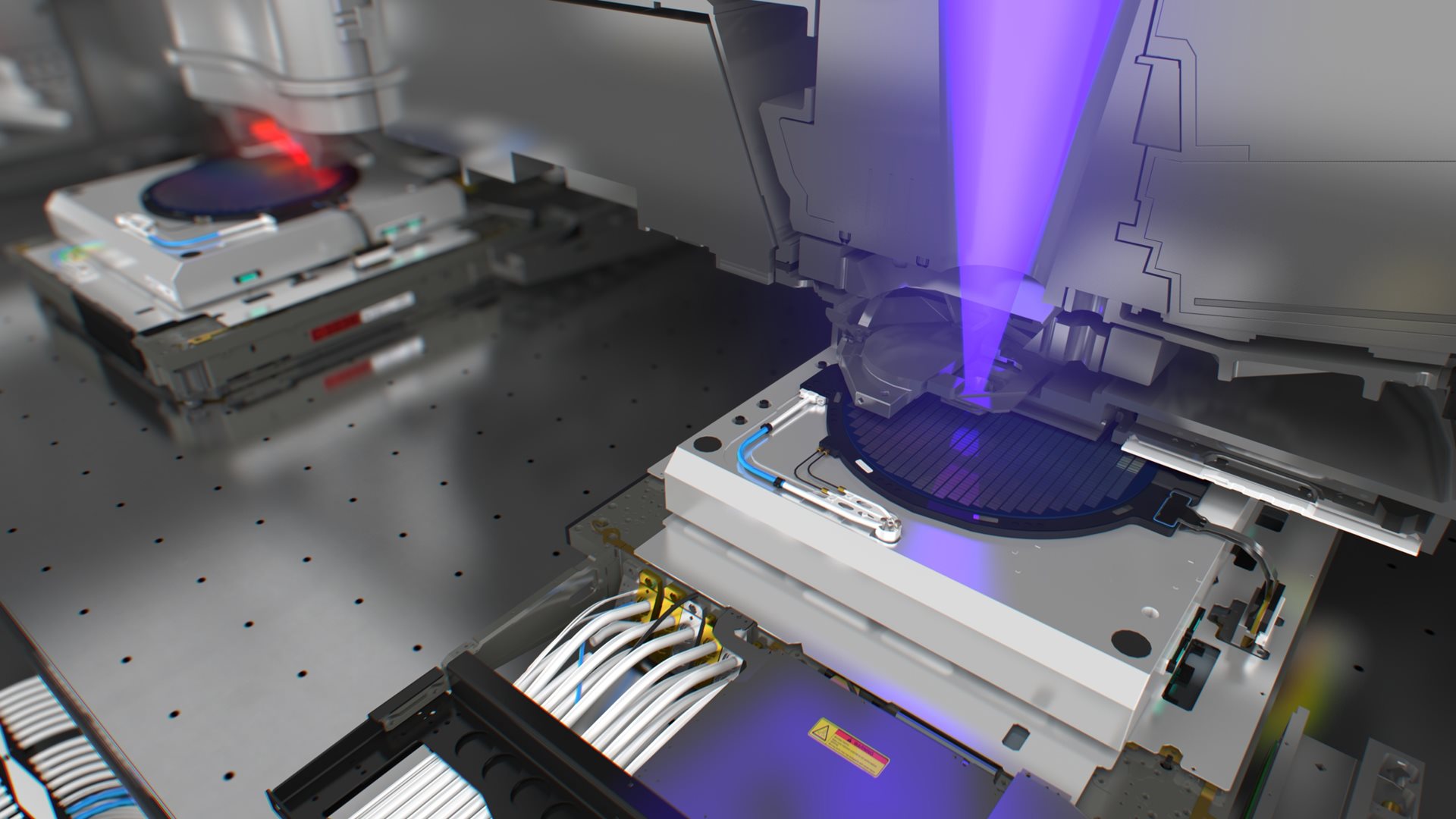
The NXE series of lithography machines will be built on an evolved TWINSCAN platform. Design of the first production system is complete, the supply chain is fully engaged and system manufacturing has started. ASML currently has orders for five of these systems from Memory and Logic customers on three continents.
“EUV lithography remains the most attractive option for extending Moore’s Law,” stated Martin van den Brink, ASML’s executive vice president of marketing and technology. “As a single-exposure, multi-node technology, EUV offers the greatest extendibility at the lowest cost of ownership.”
NXE production systems are the result of the learning and infrastructure development made possible by ASML EUV Alpha Demo Tools (ADT). In August 2006, ASML shipped the industry’s first full-field EUV exposure tools. One EUV ADT was installed at IMEC in Leuven, Belgium, and another at CNSE in Albany, New York, US.
EUV technology milestones
Both IMEC and Albany have EUV development programs being executed on ADT systems with continuously improving performance results.
- The first functional devices made using EUV lithography on full-field chips were published in February 2008.
- The contact layer of a functional 32 nm SRAM cell printed using EUV lithography was demonstrated in July 2008.
- Progress with photoresist development has yielded 28 nm half-pitch images using single exposure, conventional illumination, and no OPC (Optical Proximity Correction). OPC is a photolithography enhancement technique that modifies the chip design pattern on the mask to compensate for image errors due to diffraction.
- System overlay has been improved to 5 nm, the same distance a human hair grows in one second.
- Throughput has seen a tenfold increase since the ADT systems were first installed.
- The first prototype LPP (Laser Produced Plasma) system is operational and 100 W burst power was achieved on schedule. LPP is one method of generating EUV photons for imaging and will be used in the first NXE production systems. Discharge-produced-plasma (DPP) is another method which is currently used in the ASML EUV ADT.
- In addition to critical development work on ADT that enables EUV for production, critical technology milestones have been reached on hardware for the volume production platform.
About ASML
About EUV


