Press release - Tokyo, Japan, December 1, 2010
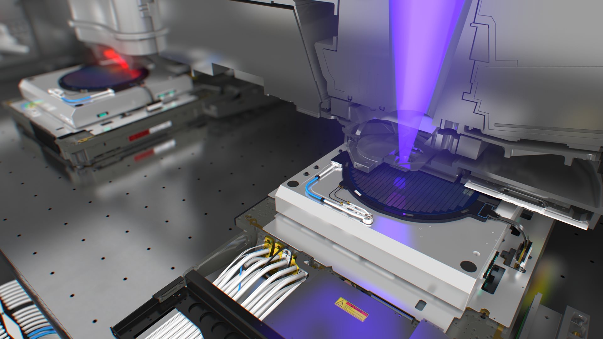
ASML Holding NV (ASML) today announced that two chipmakers using TWINSCAN semiconductor lithography scanners have set a new productivity record of imaging more than 4,000 silicon wafers within 24 hours. The milestone has been reached by an XT:870 and an XT:400, which are in operation at two different customer sites in Asia and which have raised the bar for 300 mm lithography productivity.
ASML and its customers are mutually engaged to continuously increase the value of ASML scanners by pushing to increase their productivity. ASML strives to develop improvements to scanner hardware and software while chipmakers fine-tune their chip recipes and manufacturing processes.
One key measure of this combined effort is the number of wafers processed in a single day. Another measure is when a particular scanner processes more than one million wafers in a 365 day period and joins ASML's 'million wafer club', which recognizes this highly successful ASML-customer collaboration. The first TWINSCAN system to process more than a million wafers within a year was a TWINSCAN XT:400E i-line scanner that accomplished the feat in October 2007. Now there are more than 200 scanners in the 'club', including i-line, KrF and ArF models, and more than 25 immersion tools. Additionally, a scanner recently processed the fastest million wafers so far in only 37 weeks.
"The ability of a machine as complex as a modern lithography scanner to accomplish these productivity milestones is testimony to the dedication and cooperation of both our employees and our customers," said Frits van Hout, executive vice president, and Chief Marketing Officer at ASML. "Providing customer value through high productivity has always been the goal of ASML. We will continue to improve that value through further Productivity Enhancement Packages now in development."
About ASML
About TWINSCAN
About productivity


