Press release - Veldhoven and Amsterdam, the Netherlands, June 27, 2013
ASML, the Foundation for Fundamental Research on Matter (FOM), the University of Amsterdam (UvA), the VU University Amsterdam and the Netherlands Organisation for Scientific Research (NWO) announce their intention to establish the Institute for Nanolithography (INL), which will conduct fundamental and applied research in areas that are key to unlocking innovation in the global semiconductor industry.
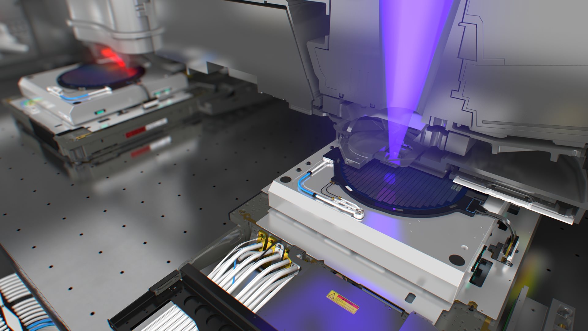
The initial research program of the INL will focus on physical and chemical processes that are key for future extensions of extreme ultraviolet (EUV) lithography. This technology is at the forefront of chip manufacturing and is indispensable for innovation in the global semiconductor industry. The institute is expected to make important contributions to semiconductor lithography, which is the key manufacturing technology for making the memory chips and processors in PCs, smartphones and tablets.
ASML will provide more than one third of the institute’s annual budget, investing roughly €30 million over 10 years. FOM and NWO will contribute €25 million over 10 years and UvA/VU will make a contribution of €12.5 million. The city of Amsterdam has committed €5 million as start-up funding. The institute is expected to benefit from the government incentive for public-private partnerships (TKI) and plans to raise €25 million from various other funding instruments such as European programs. The overall initiative amounts to €100 million for 10 years.
The institute will be launched in the third quarter of 2013 under the management of the FOM Institute AMOLF. By 2015, it will become an independent institute managed by FOM in collaboration with UvA and VU, and employ about 100 highly qualified scientists and staff, including professors, postdocs, PhD students, graduate students and technicians. The institute will be located at the Science Park Amsterdam, embedding the institute among other pioneering researchers in a stimulating environment for cooperating and exchanging ideas. The institute will be linked to the education programs of the joint science faculties of UvA and VU.
“Beyond our existing cooperation with universities and research institutes, ASML sees a need for long-term, fundamental research in nanolithography, which focuses not on making a concrete product, but on exploring technology options. This institute, with its broad research agenda, will expand the nanolithography knowledge network, contributing to innovation in the semiconductor industry,” said Martin van den Brink, ASML executive vice president and Chief Product and Technology Officer.
“The cooperation between entrepreneurs and researchers is crucial to stay at the top,” said Henk Kamp, Economic Affairs Minister of the Netherlands. “With this institute, ASML can take on the growing competition and further strengthen its global market position.”
“With this institute, we will give an important new impetus to the top sector policy in the Netherlands, aimed at increasing the impact of science on our technology base and economy. The brainstorm sessions scientists organized when preparing their proposals for this institute have already identified various research avenues, which have the potential to lead to new technology options. I am confident the institute will set an example for achieving a win-win situation for science and industry alike”, said Wim van Saarloos, director of FOM.
Jos Engelen, chairman of the Governing Board of NWO, adds: "This initiative complies with the ambition of NWO to engage in more longer-term public-private partnerships and to encourage private industry to increase its contribution to the funding of scientific research in our country. We are proud that ASML has sought this partnership with FOM/NWO."
The establishment of the new institute is conditional on contract negotiations between the partners.
About ASML
About FOM/AMOLF
About NWO
Forward-looking statements


