Press release - Veldhoven, Netherlands, February 24, 2015
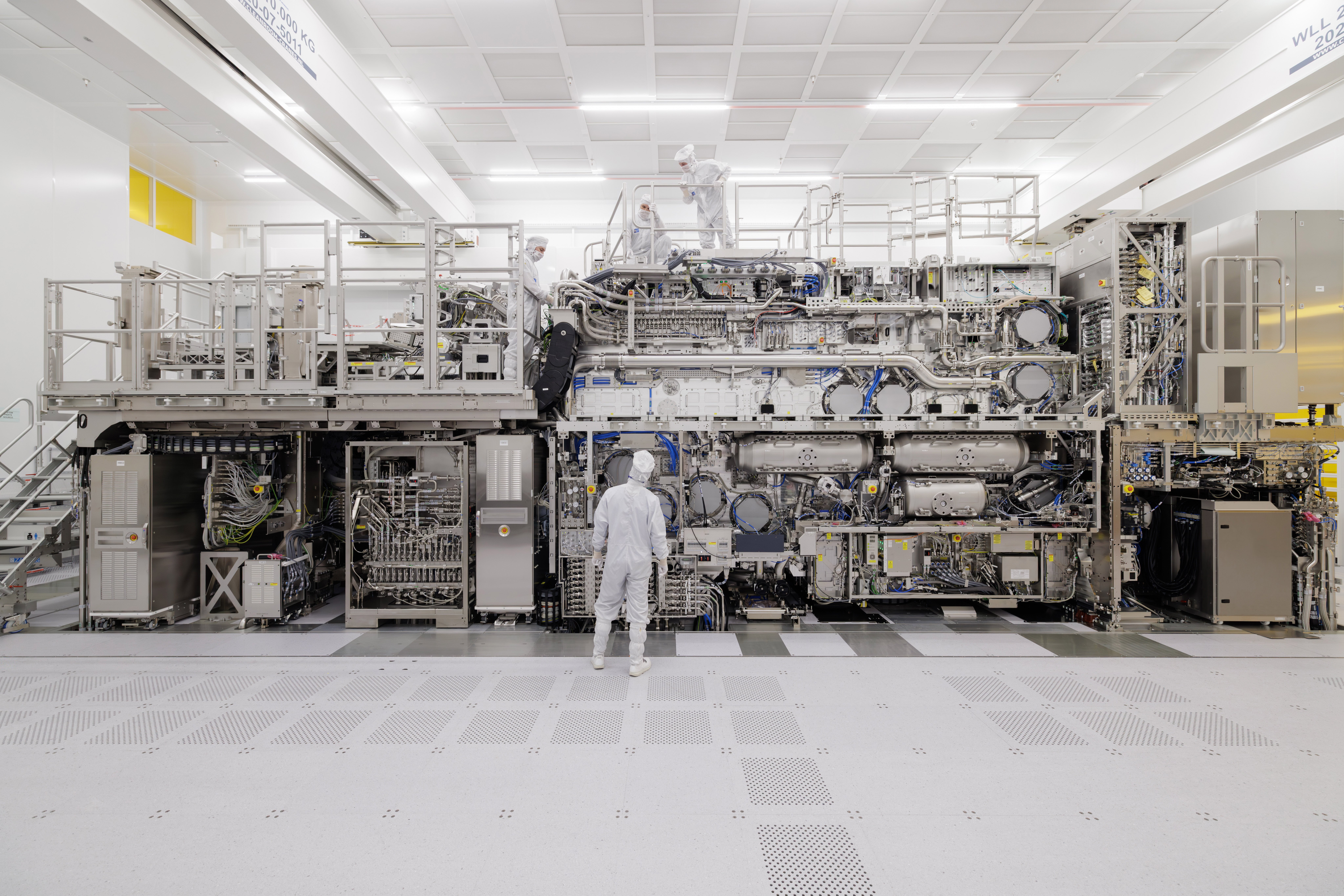
ASML Holding NV (ASML) today confirms that its customer, Taiwan Semiconductor Manufacturing Company Limited (TSMC), has successfully exposed more than 1,000 wafers on an NXE:3300B EUV system in a single day, an important step towards insertion of EUV lithography in volume production of semiconductors.
"During a recent test run on an NXE:3300B EUV system, we exposed 1,022 wafers in 24 hours with sustained power of over 90 watts," said Dr. Anthony Yen, R&D director, TSMC, at the 2015 SPIE Advanced Lithography Symposium. "We are pleased with this result, as it shows us the potential of the system."
The NXE:3300B system is one of two such systems currently at TSMC, and will be joined by two additional to-be-shipped new NXE:3350B systems. TSMC has stated that it intends to use EUV in production.
"The test run at TSMC demonstrates the capability of the NXE:3300B scanner, and moves us closer to our stated target of sustained output of 1,000 wafers per day in 2015," said Hans Meiling, vice president, Service and Product Marketing EUV, at ASML. "We must continue to increase source power, improve system availability and show this result at multiple customers over multiple days."