8-minute read - by Jorijn van Duijn, April 3, 2024
ASML was established as ASM Lithography on April 1, 1984. The joint venture from Philips and ASM International had a mandate: to commercialize a wafer stepper that had been developed at Philips, the PAS 2000.
The mythos around ASML’s founding paints a picture of a small, inquisitive startup relegated to a sticky shed and trying to break into a burgeoning semiconductor market. But how did we get to that point? Who were the early players in ASM Lithography, and why did they team up to form this new company?
This is the story of how a small project at Philips lingered at the edge of a rapidly evolving semiconductor ecosystem before finding its place, both in the industry and in Veldhoven, the Netherlands. The founding of the company was the start of something new and, at the same time, a continuation of decade-long development.
A division of labor
In the 1960s and 1970s, chipmakers built in-house the vast majority of their semiconductor value chain – all the steps needed to create a finished microchip. Then, in the late 1970s and early 1980s, the scale and complexity of semiconductor manufacturing technology grew fast. That development motivated a division of labor in the semiconductor value chain. A semiconductor equipment industry emerged to provide off-the-shelf cutting-edge solutions. With this readily available capability, it no longer made sense for chip manufacturers and users to develop their own chipmaking equipment.
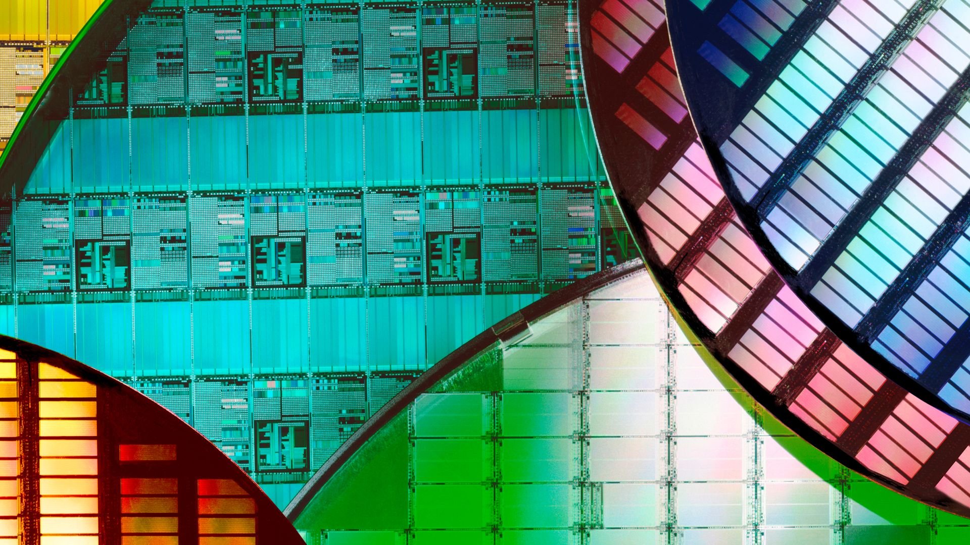
Specialized equipment suppliers were especially vital for developing the complex lithography systems used to print patterns on microchips. Improving these systems so they could print smaller features was key to driving Moore’s Law. For chip manufacturers, more transistors meant more computing power at lower cost.
This shift in the semiconductor ecosystem played out internally at large diversified companies like Philips that needed chips for a wide range of products and applications. Their in-house equipment development offered high standards. Yet, the internal Philips organization did not support the agility, adaptability and demand to mature their lithography technology to an industry-wide competitive level. Instead, large companies like Philips spun off manufacturing equipment activities in an effort to a make a buck before these technologies became obsolete.
Corporate shifts
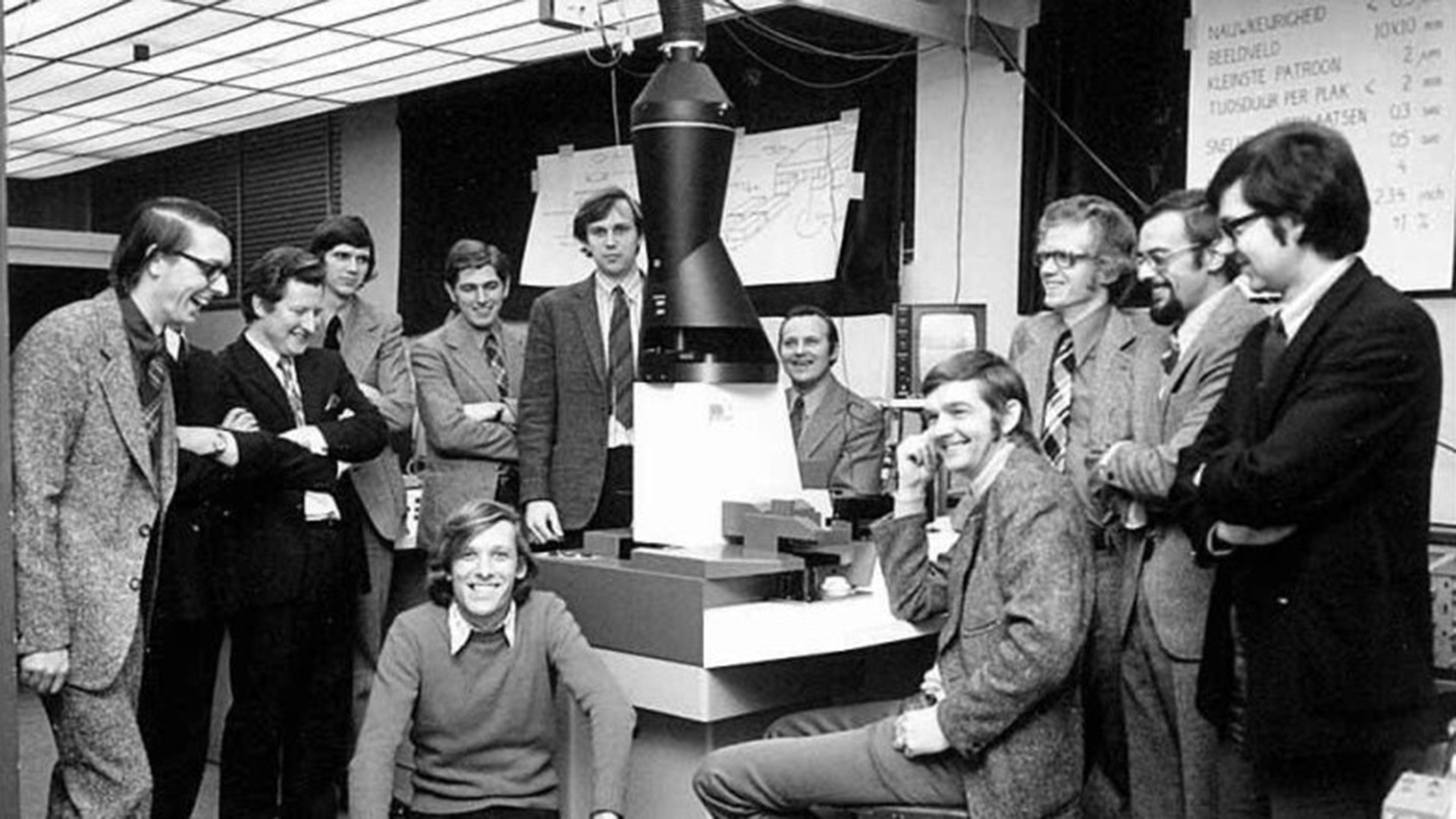
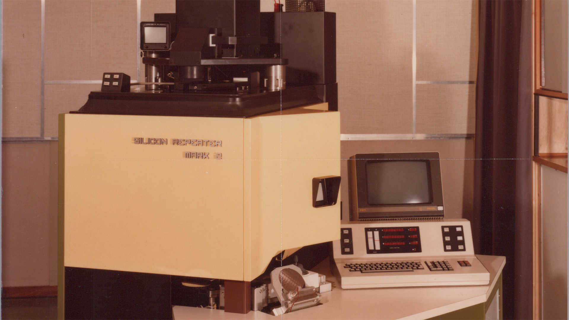
It was in this context that Philips began developing its own wafer steppers for patterning silicon wafers. The prototypes, the Silicon Repeater (SIRE) I and II, were developed by Philips Research. The Philips Automated Stepper (PAS) 2000 emerged from these research prototypes.
Within Philips Research, the division of Philips focused largely on basic research, the wafer stepper was a bit of an anomaly. Market demand was increasingly driving corporate research, and engineering manufacturing equipment was quite applied. From 1978 onwards, the Philips Science & Industry (S&I) division drove the commercialization effort under the name of PAS2000.
After the transfer from Philips Research to S&I, developing the wafer stepper became a true interdisciplinary affair. Staff from both divisions pushed and pulled to advocate for their own insights and working methods. This collaboration could clearly be seen as the first steps toward what is now known as ‘system engineering’.
Within the behemoth Philips, the PAS 2000 project was a very small activity. Still, it encountered timeline pressures and increasing costs. Facing resource scarcity, the adjunct director of S&I at the time, Wim Troost, utilized a personal discretionary budget to keep the project afloat. He also sought further support from the Philips board and the Dutch government.
After S&I took over the project, Troost and others quickly realized that the involvement of external customers was indispensable to validating the technology. They couldn’t afford to manufacture the PAS 2000 solely for internal use at Philips. If they wanted to make their lithography system, they would have to commercialize it in close collaboration with multiple customers.
Industrial policy, investors and entrepreneurs
From the late 1970s onward, guided by the
European Commission, national western European governments reshaped industrial
policies. They focused on innovation and collaboration and targeted up-and-coming
industries, in particular the rapidly expanding semiconductor industry and
microelectronics. The policies were a new means to boost economic activities
and, if possible, reviving struggling conglomerates, many of which (including
Philips) were beginning to unravel.
At the Commission’s request, Philips and
other corporate players echoed the importance of these industries to their respective
governments. Receiving this message from Europe’s largest electronics company
shaped the Dutch government’s understanding of the topic and informed their successive
actions.
Escalating costs, global competition and
technological advancements were compelling large enterprises to divest non-core
activities and refocus. For Philips, one of those activities was their wafer
stepper. At the same time, emerging venture capital firms and entrepreneurially
driven start- and scale-ups offered a new paradigm for industrial growth.

Pressure to make progress
At the start of 1982, Philips’s ambitions for a lithography product faced significant challenges. They needed more engineering resources. And although they had found an external customer, IBM, for an evaluation tool, timely delivery by the summer of 1982 was highly uncertain. Engineers from Philips Research jumped to help. S&I executives frequently visited the Hague and Brussels in pursuit of additional funding from the Dutch government and European Commission.
Under pressure of time, money and the Dutch Ministry of Economic Affairs, Philips S&I began to explore partners for its wafer stepper. This resulted in initial discussions with Cobilt, a company that made mask aligners and tracks, followed by discussions with the lithography market leader, Perkin Elmer.
Simultaneously, a trilateral dialogue emerged between the Dutch Ministry of Economic Affairs, Philips and a growing Dutch company called ASM International (or just ASM). Against the backdrop of the European Commission's novel microelectronics program, ESPRIT, chip companies had voiced concerns about their reliance on American equipment. Responding to industry needs, the Ministry and Arthur Del Prado himself proposed ASM as a potential solution.
As ASM’s founder and CEO, Del Prado epitomized the emergent and popular entrepreneurial spirit. He was a pioneer in semiconductor equipment who first brought silicon from Silicon Valley to Europe in 1958. He later made waves with an IPO on NASDAQ in 1981 – a first for a Dutch company. Del Prado’s vision and perseverance propelled his company to prominence by showcasing the transformative potential of entrepreneurial ventures in high-tech industries.
The entrepreneur eyed Philips with much interest. He was aware that the big corporations increasingly spun off innovations to reduce costs. That made their respected research labs de facto ‘incubators’. As he stated in February 1982: “I am very sceptic to make serious efforts to engage the competitors in lithography, this late, with the big boys in this area... Unless this happens together with one of the big companies like Philips…” Still, Del Prado doubted Philips executives’ willingness to collaborate in innovation.
A few months later, on October 7, 1982, Del Prado learned about the PAS 2000 project. He saw that teaming up with Philips might be his ticket into the lucrative and prestigious lithography market. Soon thereafter, the entrepreneur expressed ASM's interest for collaboration. The Ministry echoed Del Prado's sentiment, indicating the potential strategic benefits of such a partnership for the Netherlands. Such a partnership might drive Dutch capabilities in microelectronics.

Pursuing partnership
Philips, however, considered ASM too junior and favored Perkin Elmer. Despite Del Prado’s entrepreneurism and success, Philips executives regarded ASM as an upstart. Perkin Elmer – a big, diversified company with a vast installed base of lithography tools – was considered a more robust partner.
The interest was mutual. By the early 1980s, wafer steppers offered more control over the smallest feature sizes at an acceptable throughput rate than Perkin Elmer’s Micraligns. Amid heightened competition, the American company sought to swiftly secure its market position.
Perkin Elmer was considering partnering with either Philips S&I or the Liechtenstein-based startup, Censor. They preferred Philips, citing the company’s resources and the advanced nature of the PAS 2000. In the proposed joint venture, Perkin Elmer would take on a leading role, covering sales and service. Philips would contribute technology and manufacturing capabilities.
However, Philips hesitated to grant access to its internal resources, like Philips Research, in a subordinate role. This hesitation prolonged negotiations too long and, in the end, Perkin Elmer partnered with Censor.
Engineering urgency
By 1983, Philips S&I’s wafer stepper group of about 50 engineers faced uncertainty. They would need approximately 120 million Dutch guilders (about €245 million in current pricing levels) to upgrade, produce and market the machine. Despite Troost’s exhaustive and persisting efforts, including exploring partnerships with Varian and Matsushita, the wafer stepper group was out of time. The urgency was palpable.
Buoyed by positive news about ASM’s performance, S&I technical director Georg de Kruyff decided to resume discussions with Arthur del Prado in the spring of 1983. With little to lose, he and some colleagues visited ASM’s headquarters in Bilthoven, the Netherlands. Del Prado was eager for Philips’ technology and partnership, and the parties swiftly reached an agreement.

The start of ASML
Philips and ASM announced their intention for a joint venture on September 5, 1983. Over the following months they refined the partnership’s details. A stake for the Ministry of Economic Affairs or its investment vehicle was considered. Access to Philips Research was negotiated. In-kind and cash contributions were specified. Plans for a return of investments were drafted. A new ambitious and visionary general manager, Gjalt Smit, was brought on board.
Importantly, the existing group of 50 Philips S&I employees were offered attractive terms of employment. But as they already enjoyed a job for life within Philips, they considered the joint venture a form of asset stripping by Philips. There was reluctance to take a leap of faith on a start-up with no market access and whose key technology had to be redesigned. Still, 47 of the group signed on.
On April 1st, 1984, ASM Lithography commenced operations. It was initially located in Philips S&I’s Strijp TQ building in Eindhoven. The novel company, infused with fresh resources and a competitive approach, revitalized Philips’s efforts to enter the lithography market.
ASM Lithography flew out of the starting blocks. The venture was buoyed by a combination of replenished resources, a relatively high degree of autonomy, the availability of Philips’s state-of-the-art engineering practices, and an inspiring technological and commercial challenge. It rapidly added more staff, and the new employees’ enthusiasm quickly spread to the original wafer stepper team.
Business plans were drafted to upgrade the PAS 2000’s biggest drawback: its hydraulic wafer stage. Despite his dislike of using oil-based technology in semiconductor cleanrooms, Troost had chosen the mature technology over a more innovative electrical stage back in 1980. It was clear even at the time that the PAS would eventually need to be modernized. Now it was time to make that modernization a reality sooner rather than later..
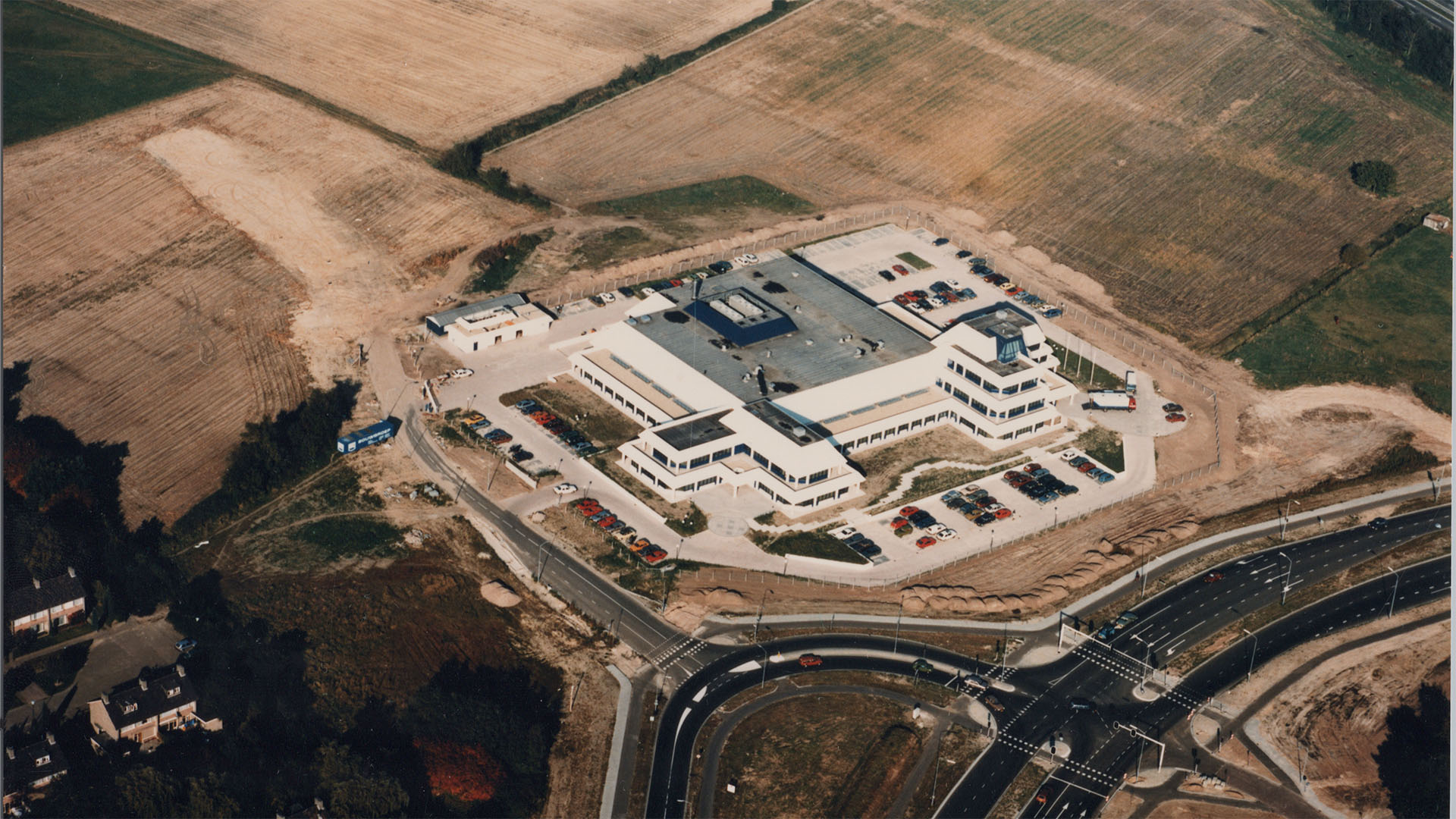
The start-up soon outgrew its facility. The problem was temporarily resolved with the addition of some uncomfortable sheds. Veldhoven was selected for the site of the permanent head office. A landmark building underlined the new company’s image and promise.
From the start, ASML was seen as the embodiment of innovation-driven entrepreneurship and having the promise to secure the Dutch economic capabilities in the future. Impetuous and ardent, the young enterprise embarked on an uncertain yet promising future.
Pushing technology forward
The move to Veldhoven may be the end of this story, but for ASML it was just the beginning. Those early days in the shed outside Philips laid the seeds for ASML to grow into the company we know today. Inventive and determined, the team pursued technical innovation that pushed the limits of what was possible.
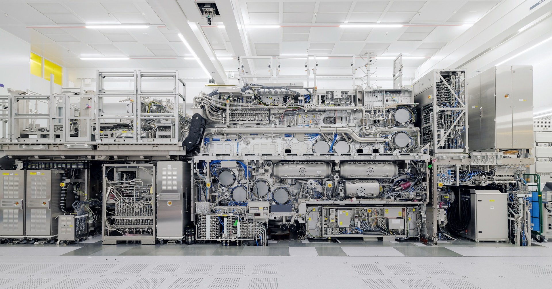
Forty years later, we’re still relentlessly pursuing groundbreaking technology. Read the rest of ASML’s story on our history page.