Press release - Veldhoven, the Netherlands, March 8, 2000
Following an extensive evaluation of lithography suppliers, SilTerra Malaysia Sdn. Bhd. has chosen ASM Lithography (ASML) as the lithography supplier to equip Silterra's new all scanner-based semiconductor manufacturing facility, scheduled to be operational by the first quarter of 2001. Critical to the success of SilTerra's operations is the lithography tool performance. After extensive evaluation of the imaging technology and productivity performance for both i-line and deep UV, high numerical aperture (NA) scanner systems, SilTerra selected ASML's PAS 5500/400 i-line and PAS 5500/700 deep UV Step & Scan systems.
"ASML has demonstrated high productivity and critical layer imaging performance with their PAS 5500 scanners, which we require to provide the most advanced design rules, process capabilities and competitive pricing for our customers," stated K.C. Ang, vice president of operations for SilTerra.
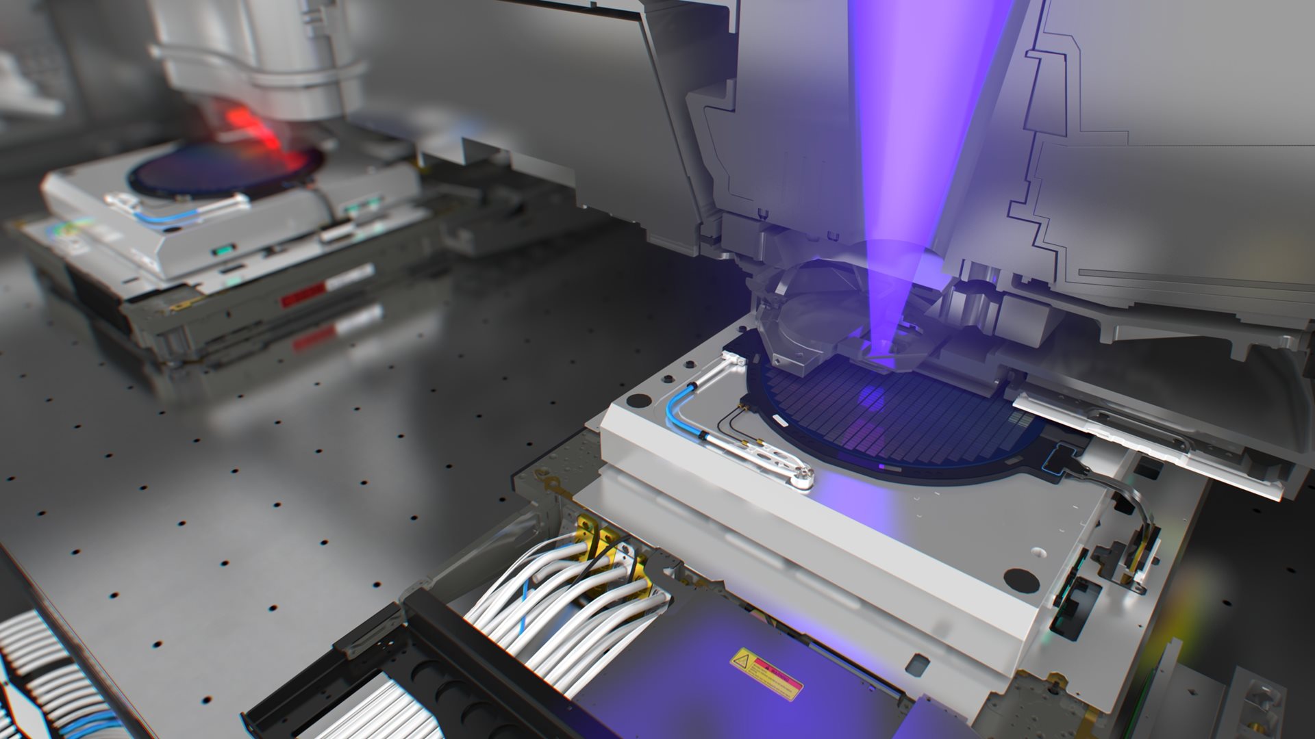
The PAS 5500/700 deep UV scanner has the highest NA (0.70) available in the industry, and when combined with ASML's patented high-intensity AERIAL illuminator, provides high-volume throughput of 120 wafers per hour with production resolution of 150 nm. The PAS 5500/400 is the industry's first i-line Step & Scan system, optimized to match the PAS 5500/700 system, which allows manufacturers to use lower-cost i-line processes for less critical layers without sacrificing wafer throughput and factory productivity.
"The PAS 5500 technology platform has been recognized as a productivity benchmark by the world's leading foundry and memory IC manufacturers, where cost-effective operations are paramount to business success. We are pleased that SilTerra, after a very thorough evaluation, has recognized our technology leadership and chosen ASML as a key supplier for their business," stated Dave Chavoustie, ASML executive vice president of sales.
About SilTerra
About ASML


