Press release - Veldhoven, the Netherlands and San Diego, California, US, July 13, 2009
ASML (Nasdaq: ASML) and Cymer, Inc. (Nasdaq: CYMI) formally announce the shipment of the world's first fully integrated laser-produced plasma (LPP) Extreme Ultraviolet (EUV) lithography source to ASML. Cymer's EUV source, the first of a multi-unit purchase agreement between the two companies, is currently being installed at ASML's Veldhoven headquarters where it will support integration and testing of next generation EUV lithography scanners.
Together with this shipment, Cymer announces achieving a record milestone of 75 watts of EUV lithography exposure power (full die exposure) and expects to scale to 100 watts exposure power within the current quarter, enabling scanner throughput of 60 silicon wafers (300 mm/12 inch) per hour which is required for volume manufacturing with ASML's EUV technology. First shipments of production-capable EUV scanners from ASML are planned a year from now. The source concept will be capable of scaling over time to performance levels consistent with exposing more than 100 wafers per hour when fully integrated into ASML scanners.
EUV is a new lithographic method using a 15 times shorter wavelength than current lithography systems, enabling semiconductor scaling to resolutions of 10 nanometers (nm) and smaller. EUV will support Moore's law – the trend towards more powerful, energy-efficient yet affordable chips – for at least another 10 years.
"Our team has worked hard to ship the industry's first LPP EUV lithography source while achieving new levels of EUV power," said Bob Akins, chief executive officer of Cymer. "We are pleased to be partnering with ASML in the advancement of EUV lithography, which will offer high-resolution, high-throughput, manufacturing capability for the production of advanced ICs with critical dimensions below 22 nm, enabling the continuation of Moore's law for multiple chip generations to come. Within the next few years, chips patterned by EUV lithography will be hundreds of times more powerful than today's," concluded Akins.
"Cymer and ASML are committed to bringing EUV lithography to production reality for chip makers worldwide," added Martin van den Brink, Executive Vice President of Products and Technology at ASML. "EUV is by far the most cost-effective volume lithography technology for more powerful future generations of semiconductors, and our achievements show how the equipment industry is making huge strides to the introduction of the first production-ready EUV lithography tools in 2010. This revolutionary new architecture provides chip makers with technology that will extend the semiconductor shrink for another decade at least."
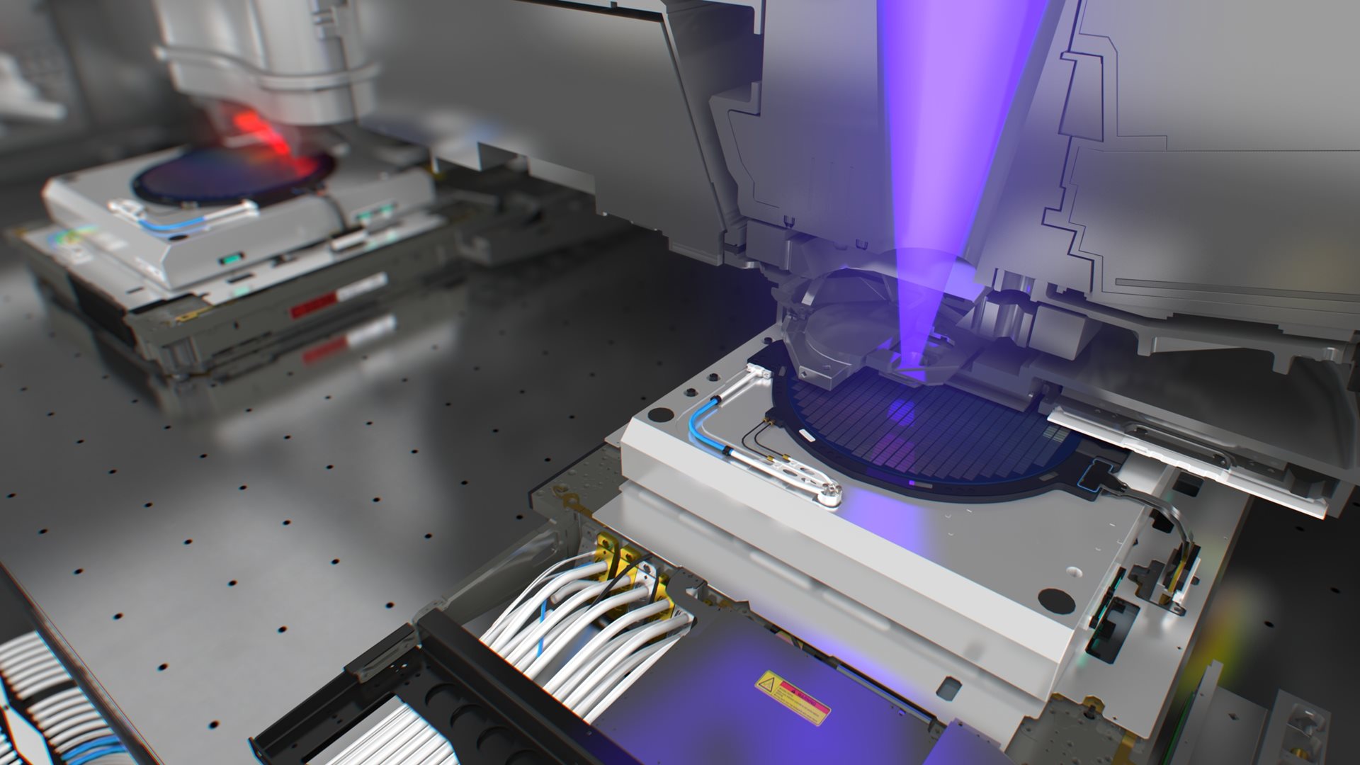
An LPP EUV lithography source, which produces "light" with 13.5 nm wavelength (invisible to the human eye), represents a significant technology paradigm shift from today's Deep Ultraviolet (DUV) lithography excimer laser sources. In an LPP EUV source, microscopic droplets of molten tin are fired through a vacuum chamber and individually tracked and vaporized by a pulsed high power infrared laser – as frequently as 50,000 times per second – creating a high temperature tin plasma point source which radiates 13.5 nm wavelength light. A large EUV mirror collects and directs this light into the scanner where it is patterned by a photomask and projected using a complex set of image reduction mirrors onto a light-sensitive silicon wafer – transferring the pattern onto the wafer.
ASML has received orders for five EUV lithographic systems from memory and logic customers on three continents, with deliveries starting in 2010.
Forward-looking statements
Statements in this press release that are not strictly historical in nature are forward-looking statements. These statements include, but are not limited to the development and potential benefits of EUV lithography and continuing advancements in IC manufacturing; the capabilities of future chips, including the continuation of Moore's Law; and pending orders for EUV systems. These statements are based only on current information and expectations that are inherently subject to change and involve a number of risks and uncertainties. Actual events or results may differ materially from those projected in these statements due to various factors, including but not limited to: the risks inherent in developing new technologies; cyclicality in the semiconductor equipment industry; the demand for semiconductors in general, and, in particular, for leading-edge devices with smaller geometries; the rate at which semiconductor manufacturers take delivery of photolithography tools; delays or cancellations by customers of their orders; new and enhanced product offerings by competitors; the timing of customer orders, shipments and acceptances; inability by the company to meet its production or product development schedules; and inability of the company to secure adequate supplies of critical components for its advanced products. For a discussion of these and other factors which may cause actual events or results to differ from those projected, please refer to Cymer's most recent annual report on Form 10-K and ASML's most recent annual report on Form 20-F, as well as other subsequent filings with the Securities and Exchange Commission. You are cautioned not to place undue reliance on these forward-looking statements, which speak only as of the date of this press release. All forward-looking statements are qualified in their entirety by this cautionary statement, and neither ASML nor Cymer undertakes any obligation to revise or update any forward-looking statements to reflect events or circumstances after the date of this press release.
About ASML
ASML is the world's leading provider of lithography systems for the semiconductor industry, manufacturing complex machines that are critical to the production of integrated circuits or chips. Headquartered in Veldhoven, the Netherlands, ASML is traded on Euronext Amsterdam and NASDAQ under the symbol ASML. ASML has more than 6,500 employees, serving chip manufacturers in more than 60 locations in 15 countries.
About Cymer
Cymer, Inc. is the market leader in developing light sources, used by nearly every major chipmaker around the world as the essential light source for DUV lithography systems. With numerous offices worldwide and company is headquartered in San Diego, Calif. Cymer's newly launched DUV sources enable double patterning techniques that could be used to pattern wafers with critical dimensions as small as 22nm. The company is also leading the industry in the development and transition to LPP EUV lithography sources. Cymer is committed to developing and introducing new technologies that improve the capability, productivity, and cost of ownership. Cymer maintains a Web site to which it regularly posts press releases, Securities and Exchange Commission report filings, and additional information about Cymer. Interested persons can also subscribe to automated e-mail alerts or RSS feeds. Please visit www.cymer.com.


