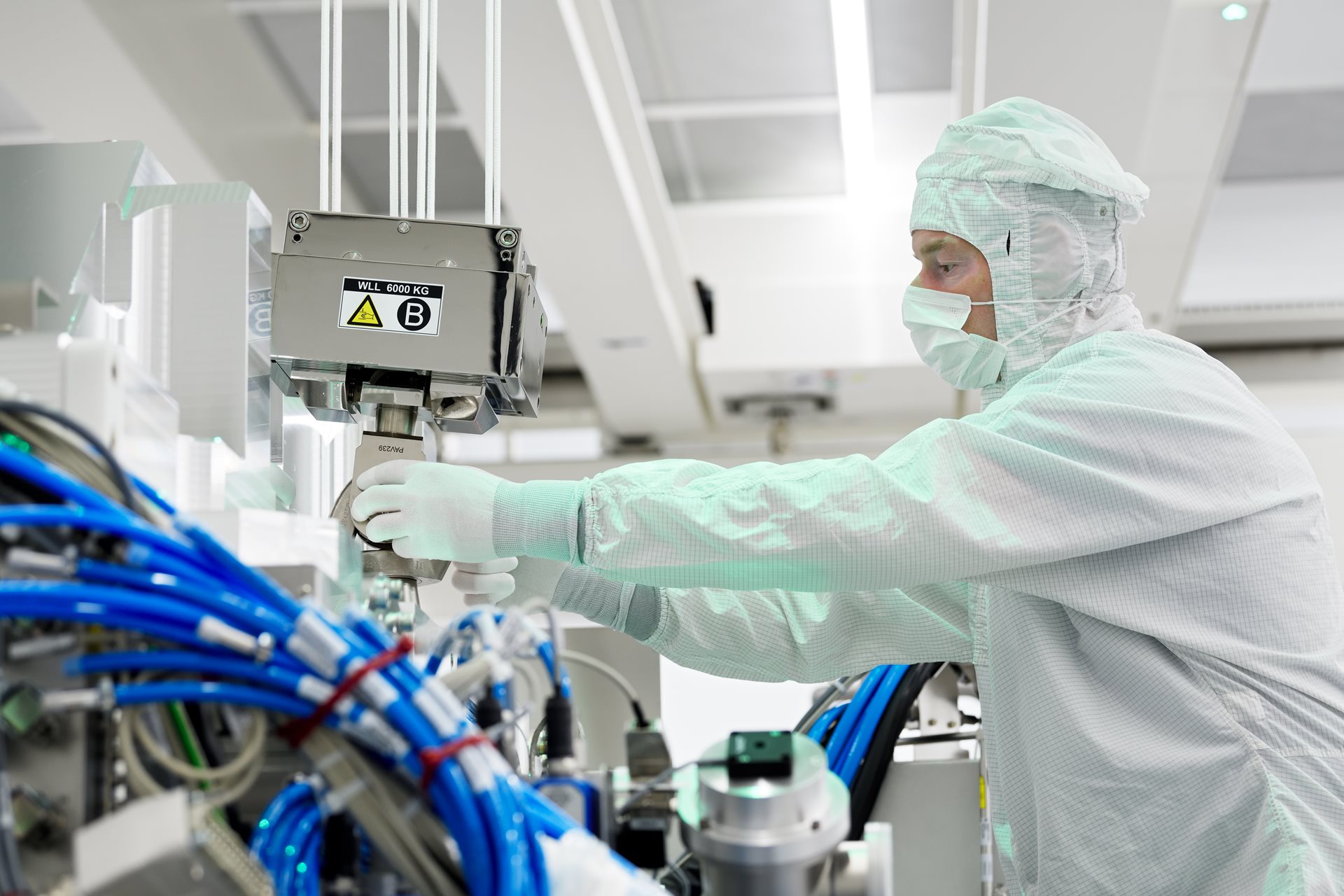
Delivering holistic lithography value
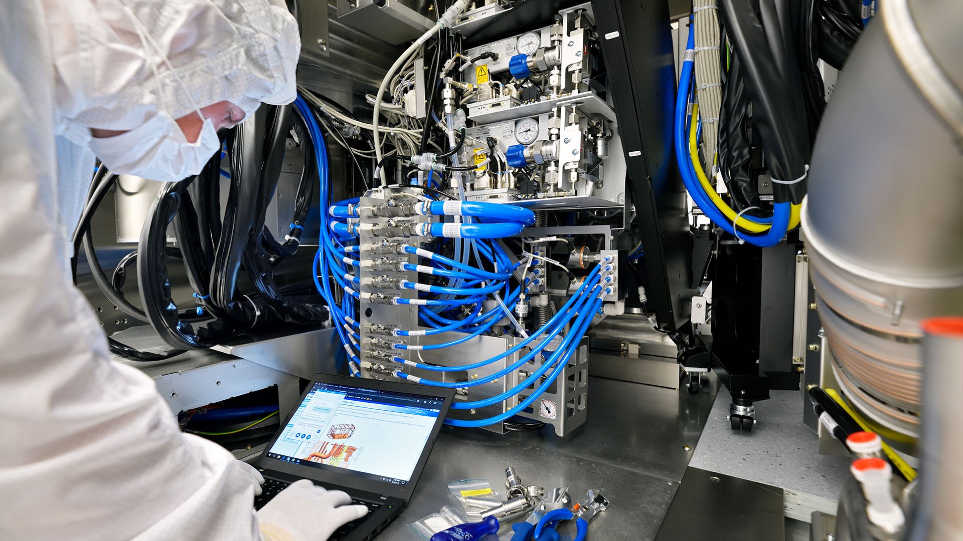
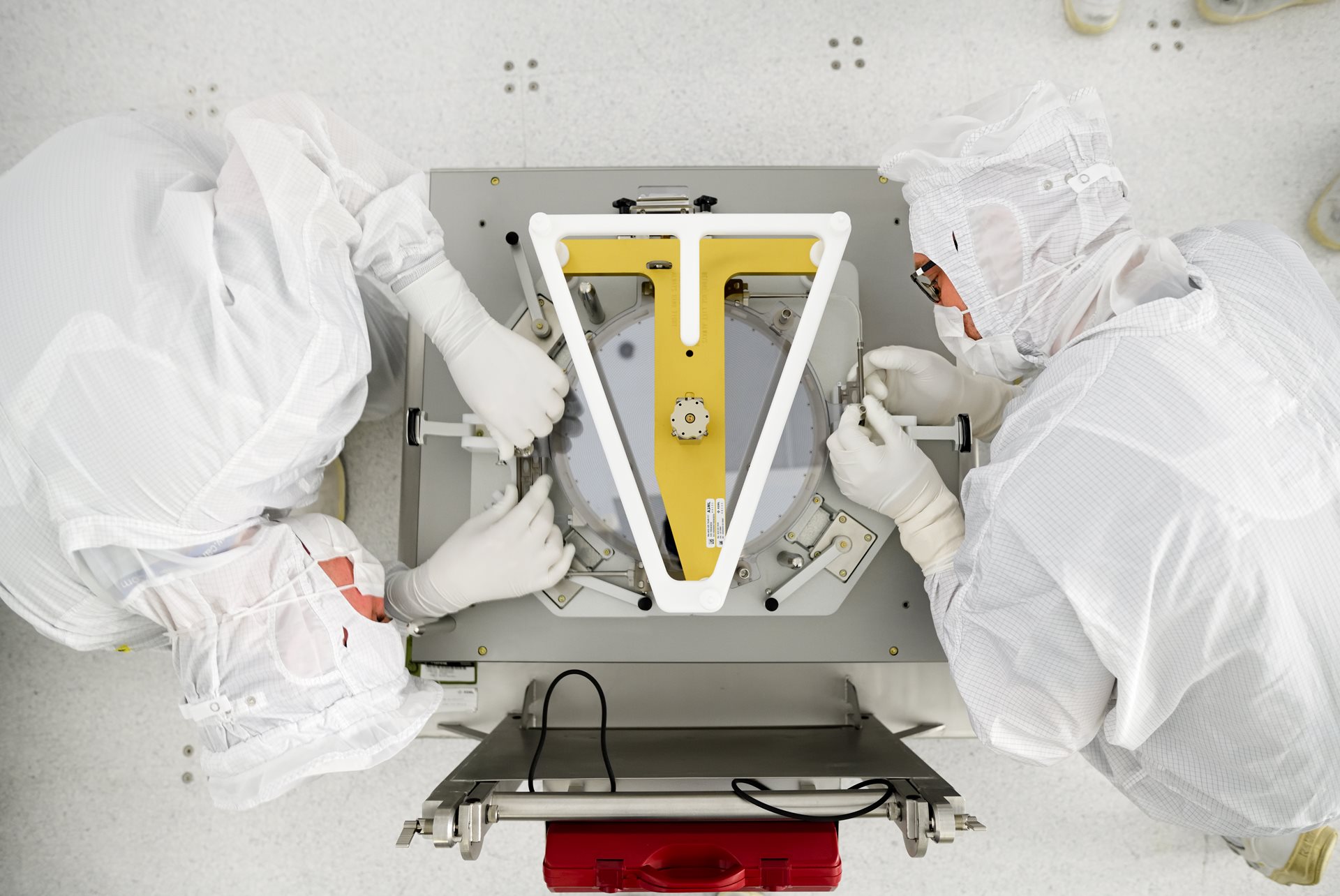
At ASML, we provide our customers with everything they need to mass produce microchip patterns on silicon wafers. Our holistic approach integrates computational modeling, optical metrology and e-beam inspection with lithography systems so chipmakers can meet their most stringent patterning requirements and optimize their chipmaking processes quickly and at the right cost.

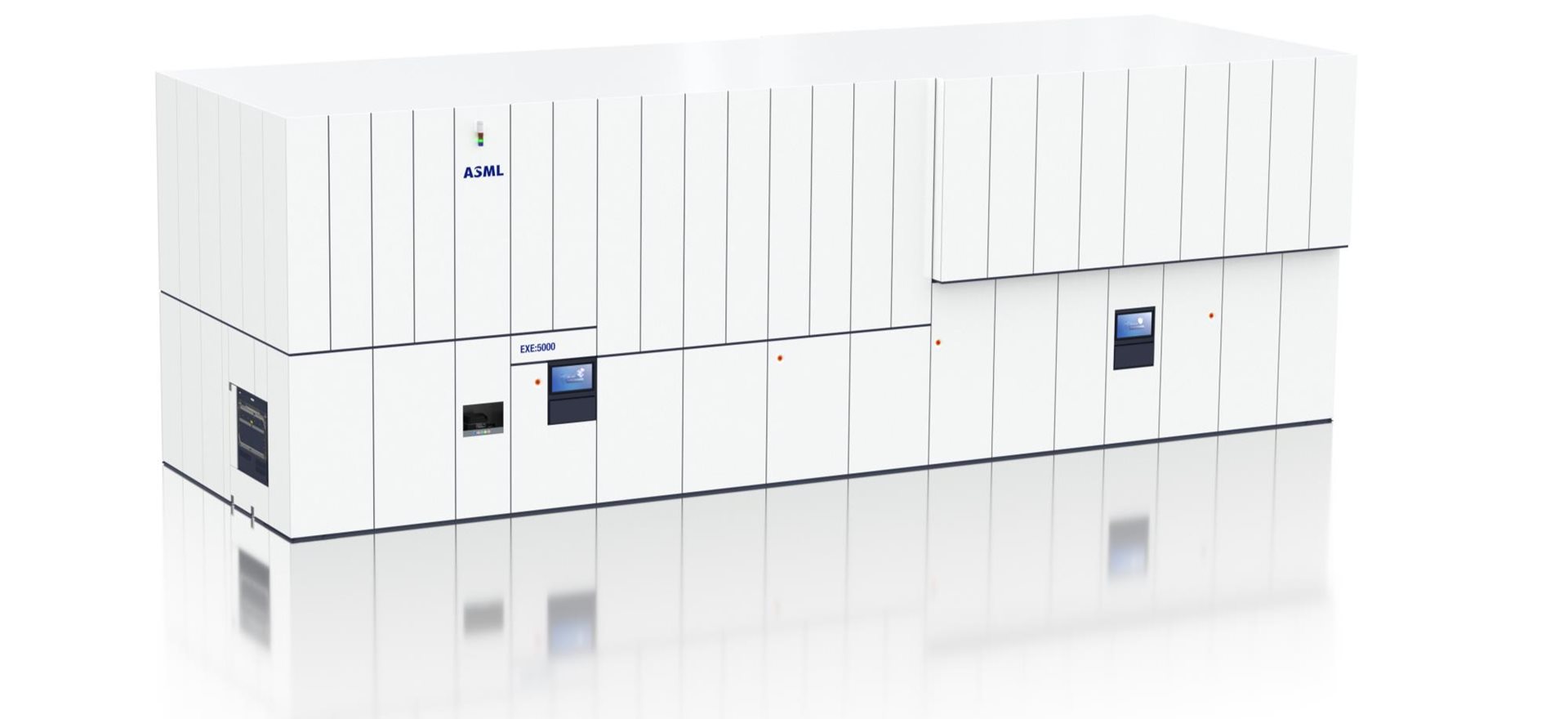
EUV lithography systems
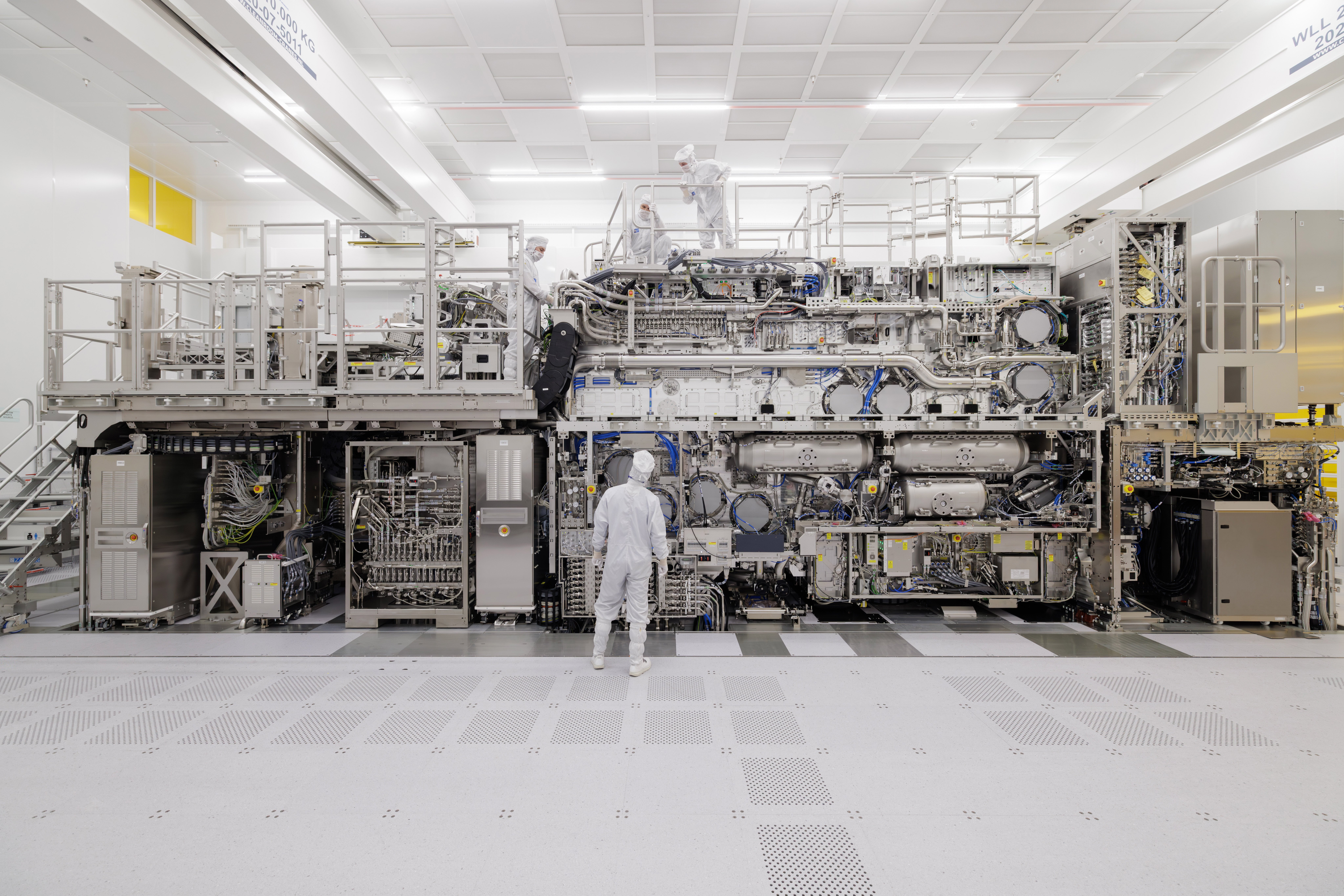
Our extreme ultraviolet (EUV) lithography systems provide the highest resolution in high-volume manufacturing. By enabling chipmakers to squeeze even more transistors onto a single chip, the state-of-the-art technology – which is unique to ASML – is pushing Moore’s Law forward.
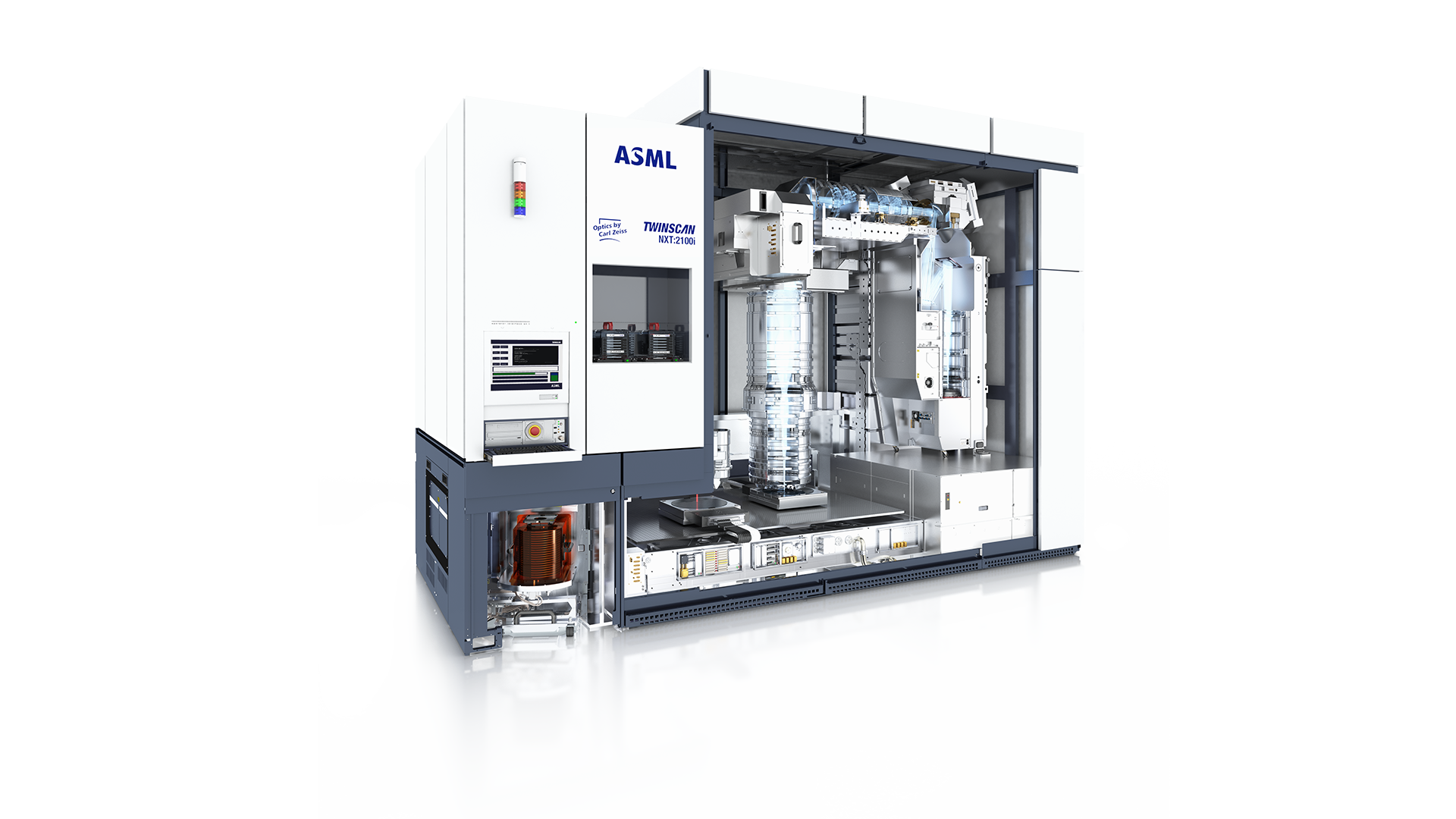
DUV lithography systems
Deep ultraviolet (DUV) lithography systems are the cornerstone of the semiconductor industry. The dry and immersion DUV systems in our portfolio are used for high-volume manufacturing of the most advanced Logic and Memory chips, novel chip innovation and everything in between.
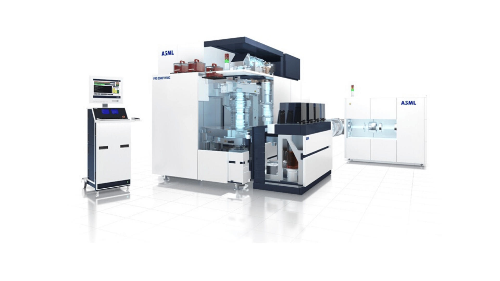
Refurbished systems
Almost every lithography system that we’ve ever shipped is still in use at a customer fab. We refurbish ‘classic’ PAS 5500 and TWINSCAN lithography systems for a new life and a new purpose.
Metrology & inspection systems
Delivering speed and accuracy, our metrology and inspection portfolio covers every step in the chip manufacturing process, from R&D to mass production.
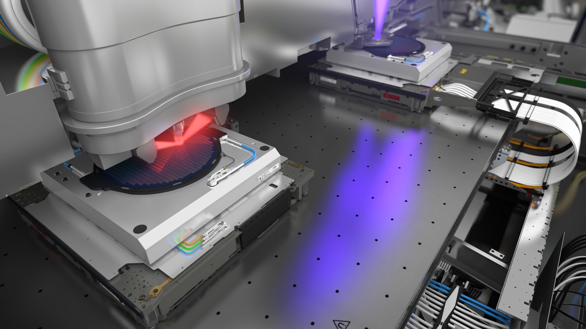
Computational lithography
ASML is pioneering this industry-leading technique, which minimizes the physical and chemical effects that interfere with the quality of a chip.
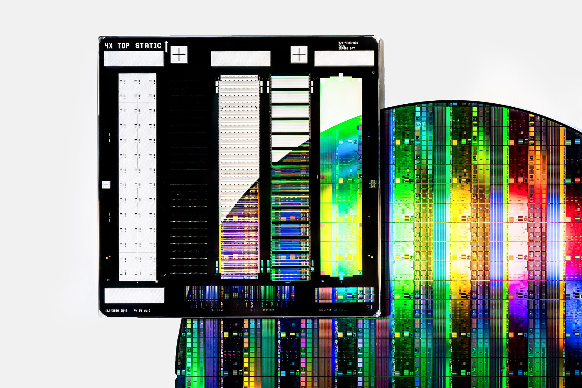
Customer support
At ASML, the customer always comes first. With around 10,000 customer support employees, including service engineers and applications specialists, we make sure our systems in our customers’ fabs are running smoothly.