In 1965, Intel co-founder Gordon Moore observed that the number of transistors on a microchip was increasing rapidly. He foresaw that this exponential increase in computing power would be the key to affordable electronics manufacturing.
Moore predicted that the number of transistors in a microchip would double every year for the next decade. In 1975, he revised the prediction to every two years. His prediction, known as Moore’s Law, has proved to be true – or, as some argue, a self-fulfilling prophecy. The number of transistors that can be squeezed on a chip has grown from tens in the 1960s to tens of billions today.

A driver of progress
Moore’s Law has propelled the semiconductor industry forward. For chipmakers, being first to market with a new generation of smaller, denser, more powerful chips has proved lucrative. And, thanks to scaling, the cost of Logic and Memory chips has dropped so dramatically that it’s now possible to put a chip in practically anything. As we move from a world where microchips are everywhere to one where AI is everywhere, the growth opportunities for the industry will only continue to expand.
The relentless pace of Moore’s Law has changed the world we live in. By repeatedly doubling the number of transistors on a chip, chipmakers keep delivering higher performance at lower cost with each new generation of chip. The result? Consumer products that were once the stuff of dreams.

Moore’s Law is alive and well
Innovation doesn’t slow when transistor shrink does. It just becomes more challenging – and, as a result, more profitable if done well.
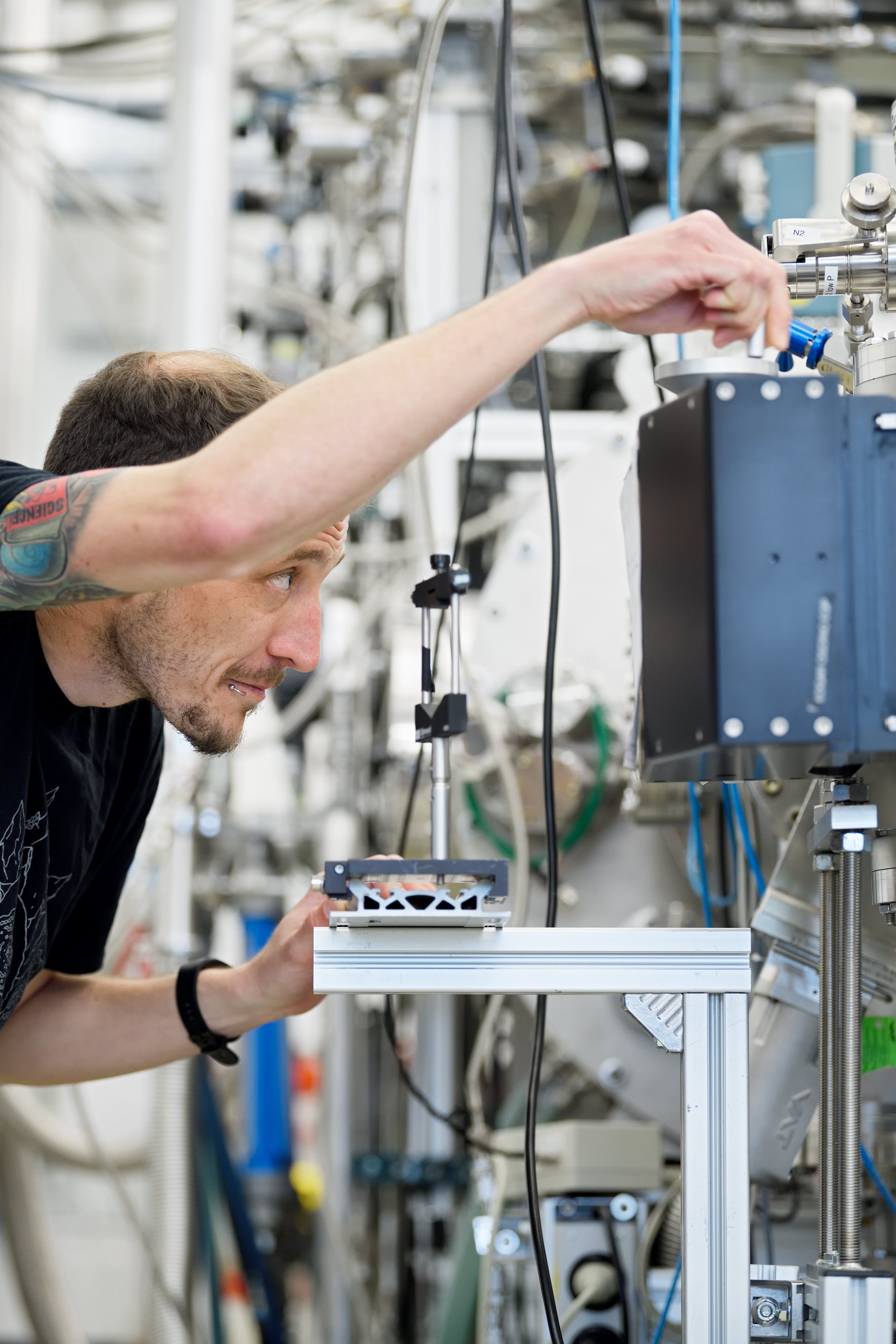
As the pace of 2D shrink slows, chipmakers are relying more and more on exotic materials, advanced packaging technologies and more complex 3D transistor designs to deliver improved chip performance. The semiconductor industry increasingly needs to connect engineers from across the entire breadth of physical, chemical, biological and computer sciences in order to realize their new designs – designs that will change our technological world in ways that right now we can’t even conceive of. They will enable waves of innovation in areas such as autonomous vehicles, hyperconnectivity, medical technology and – perhaps most impactfully – the spread of faster, more efficient AI into every aspect of our lives.
Enabling progress with holistic lithography
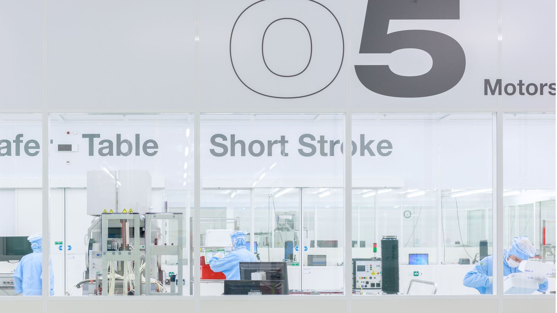
What will always be needed is a way to mass produce chips at the right cost. That’s where holistic lithography – the integration of lithography with metrology, inspection and computational lithography – comes in. Our products work together to maximize lithography performance and ensure affordable shrink.
We continue to push the productivity and imaging performance of our lithography machines, with EUV lithography providing the highest resolution to enable tomorrow’s most advanced chips. That precision patterning is supported by our metrology and inspection systems, whose capabilities we’re continually expanding to meet the demands of today’s complex 3D chip architectures. And in our computational solutions, machine learning and big data will continue to help us better model both lithography and metrology processes with high accuracy, helping chipmakers optimize their manufacturing for highest performance at the lowest cost.