5-minute read - by Brittney Wolff Zatezalo, October 23, 2020
For many decades, manufacturing was intensive manual labor: clock in, follow instructions, get your hands dirty, and clock out. To celebrate Manufacturing Month in the US, we’re taking an inside look at the unique world of manufacturing at ASML.
Modern-day manufacturing is nothing like the dirty, greasy images from the industrial age. The arrival of the integrated circuit (or chip) enabled automated production as well technological evolution. And, as author Simon Winchester says in his book The Perfectionists: How Precision Engineers Created the Modern World, “the leading edge of precision passed itself out into the beyond, moving … from the purely mechanical and physical world and into an immobile and silent universe, one where electrons and protons and neutrons have replaced iron and oil and bearings and lubricants.”
What is high-tech manufacturing?
This is the manufacturing world of ASML – called semiconductor equipment manufacturing. We research, design and build machines that are not only very precise but also function at incredible speed and velocity. Our lithography machines can print nanoscale circuit patterns on silicon at a rate of over 250 wafers per hour. For average phone-size chips, that’s hundreds of thousands of chips per hour. And chips are still getting smaller and more advanced – as seen in the chip in the new iPhone 12, made possible by ASML.

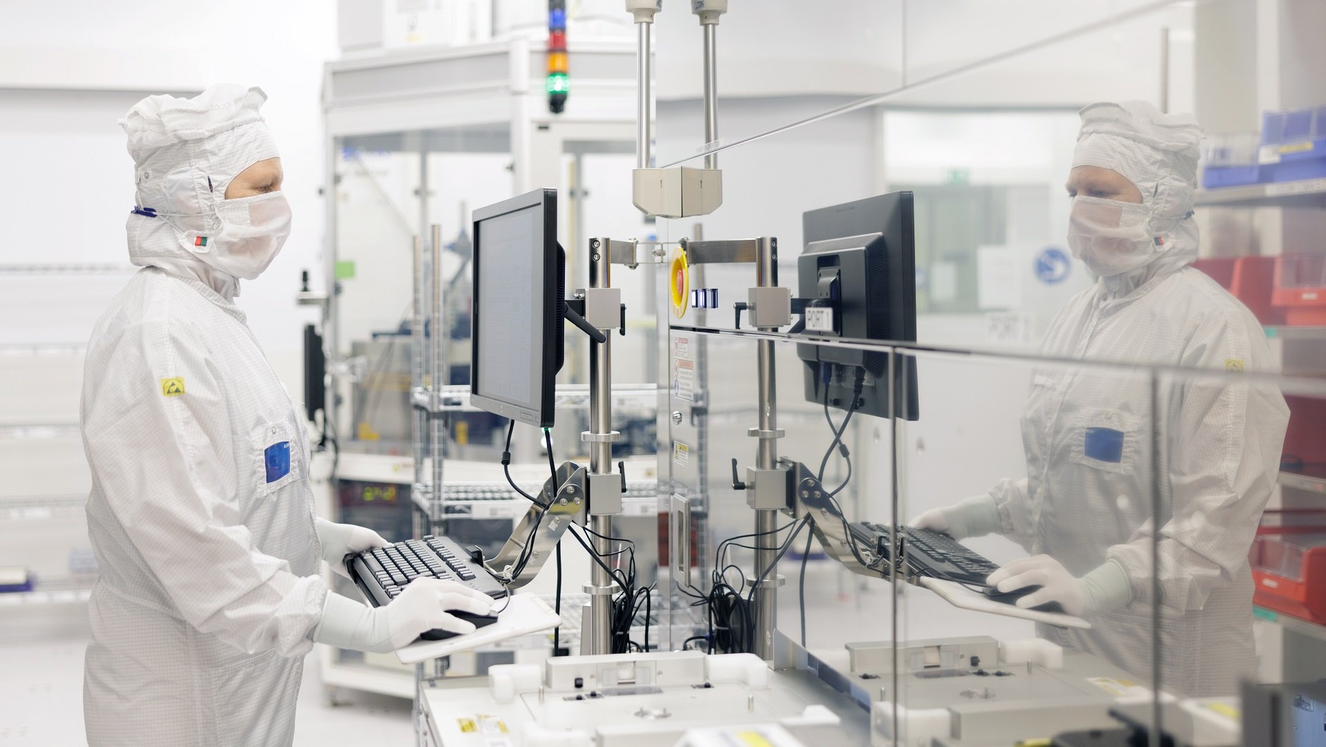
Cleaner than clean
These machines don’t need oil and grease to keep production going – they actually need the opposite. Our manufacturing facilities are called ‘cleanrooms’ because cleanliness is their most important feature, measured using internationally agreed standards (ISO) of cleanliness to quantify particulates.
For example, at Goddard Space Center in Maryland, the cleanroom where NASA engineers assembled the James Webb Space Telescope is classified as an ISO 7 environment. This allows 352,000 half-micron-size particles in every cubic meter of air. ASML cleanrooms in the Netherlands, however, abide by the ISO 1 standard, allowing only 10 particles of just one-tenth of a micron per cubic meter, and no particles of any size larger than that.
It’s strict because it has to be. A single particle of dust can be catastrophic in the chipmaking process. If even the smallest speck of dust lands on the chip pattern, once light passes through and is reflected onto the silicon wafer, it becomes a large spot that renders the chip completely useless. By the time it is discovered, hundreds of chips will have been ruined.
In our cleanrooms, workers gown up from head to toe in special ‘bunny suits’ – looking like high-tech manufacturing astronauts – to ensure they don’t introduce any dirt into the environment.
The difference is in the details
High-tech manufacturing at ASML requires an incredibly diverse group of individuals – from engineers and designers to technicians, opticians and assemblers – to successfully go from a design to mass production.
“Imagine the mechanical or electrical aptitude you need to look at a drawing and intuitively know how to put together the right team of technicians and production and manufacturing engineers to assemble a product with very precise specifications,” Jim Love, who leads the ASML San Diego factory, explains. “Or the skill and attention to detail needed to bring every part from the supply chain within a couple square meters at the precise time needed for the team to complete the build.”

ASML has five manufacturing locations worldwide. Our lithography systems are assembled in cleanrooms in Veldhoven, the Netherlands, while some critical subsystems are made in different factories in San Diego, California, and Wilton, Connecticut, as well as other modules and systems in Linkou and Tainan, Taiwan.
Each factory specializes in a different area. The Wilton site, for example, consists of two manufacturing competencies: 1) assembly and test to build and qualify various subsystems for the scanner and 2) optical fabrication to produce all different types of glass and ceramic structures.
Wilton specializes in making extremely low-aberration optical elements used in ASML’s scanners and metrology systems that enhance measurements to enabled improved control of key patterning parameters for chipmakers. Optical elements are polished within two orders of magnitude more precise than eyeglasses, which requires very advanced measurement tools that only a few companies in the world have and use.
“The challenge in our optical fab is that the process is not absolute. The team needs to tap into their inherent skill set, knowledge and experience – applying science into an amazing art form,” says Guido Capolino, who oversees optical production.
Meanwhile, the San Diego’s factory output looks completely different. Here the team specializes in making several critical modules within the droplet generator – the heartbeat of the EUV source. This includes a nozzle, which is made with robotic equipment that melts, polishes, dissolves and glues glass – transforming something that looks like a straw into a highly precise funnel with an opening that is +/- 500 atoms wide.
Regardless of the specialty, all of ASML’s high-tech manufacturing sites are connected by one common and paramount requirement – extreme precision. Our assemblers and technicians work within micron-level parameters equivalent to the width of a human hair.
An entirely new skill set
High-tech manufacturing requires a workforce with computer programming knowledge, an aptitude for mathematics, and precision machining experience. The work is detail oriented – there is no room for mistakes.
With all the different competencies required for mass production, there are endless opportunities to grow and pivot your career within the manufacturing team, if you have the drive to challenge yourself and a growth mindset to learn new skills.

“The beauty of working in manufacturing at ASML is that no area is off limits,” says Jim. “There’s freedom to move with your interests in high-tech manufacturing, where your own ambition is the only limitation. I really like making something. I have a big sense of pride when I see the truck rolling away with a physical product on it and I was a part of making that happen. It’s not just an exercise of the mind on paper – rather it’s the physicality of making all the parts come together into a functional product that is essential to enabling our customers to manufacture the silicon chips we rely on every day.”
The future of manufacturing at ASML is bright! Learn more about high-tech manufacturing jobs at ASML.