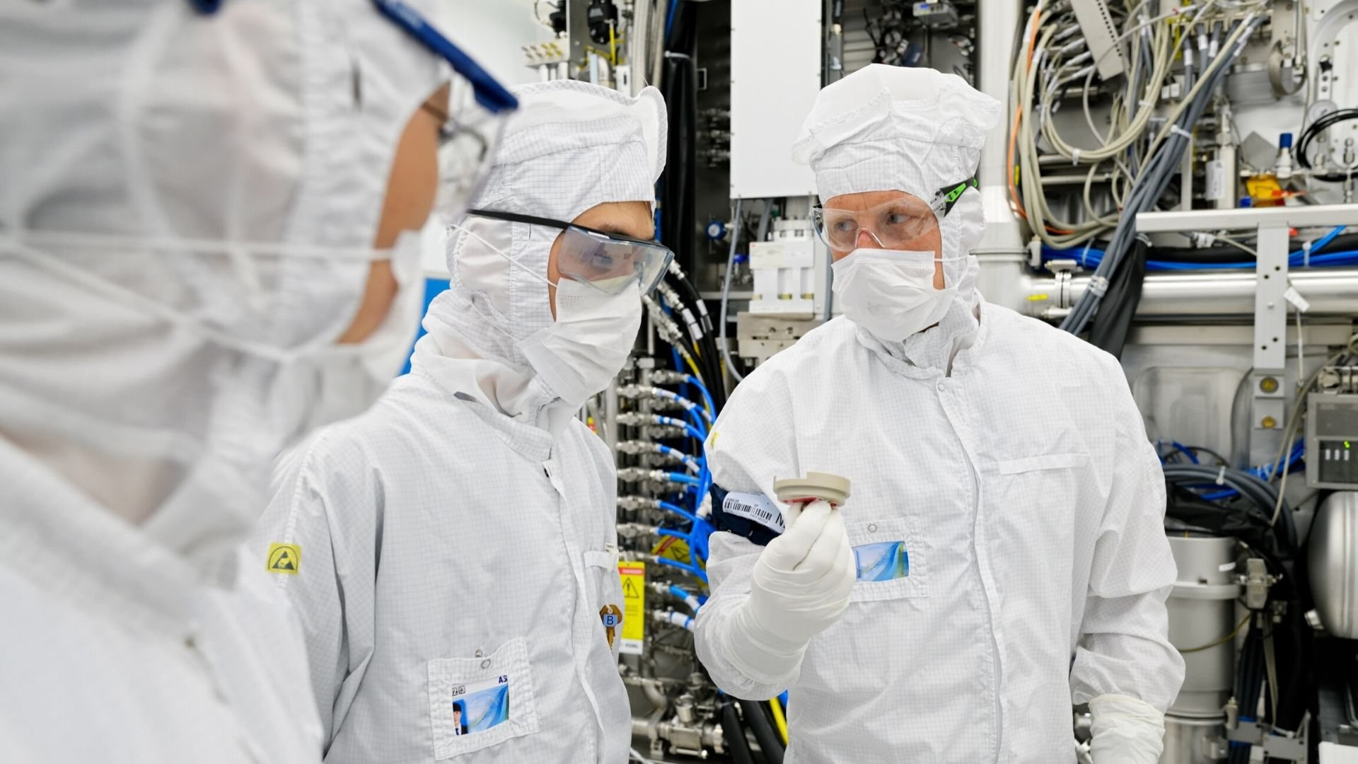
4-minute read - by Sue Todd, May 23, 2021
Imagine you are asked to build the world’s tallest skyscraper. On uneven land. With no room for error and every story aligning perfectly with one another. Oh, and you have to do this all on the nanometer scale. Sound impossible? ASML’s engineers face this challenge every day with 3D NAND chips – but they are making them a reality through our expertise in an area known as scanner metrology.
3D NAND is a type of microchip with non-volatile memory, also known as flash memory, which supports high-performance electronics and innovations such as automated vehicles, advanced AI and 5G connectivity. It is made of stacks of memory cells placed on top of each other in order to create a multi-story, 3D-chip structure.
This relatively new type of chip design addresses the challenge of the limited amount of bits that can fit on a two-dimensional cell. A 3D NAND chip is able to hold more bits, run more efficiently and use less energy than their 2D counterparts. But it is more difficult to make.
A 2D microchip goes through hundreds – sometimes thousands – of different processes to make just one layer of a working device. This year, 3D NAND chips that have 176 layers were released, so it’s no surprise that fabricating these chips requires an even more intricate production process.
Precision and alignment
The crux of this challenging undertaking is to ensure the stack of layers is constructed uniformly and aligned with sub-nanometer precision to then be connected using tiny vertical channels. Alignment is an integral part of printing chip patterns on wafers, and for 3D NAND the pressure is ramped up.
“Instead of making bungalows, we’re now making multi-story skyscrapers. As you can imagine, this is a highly complex undertaking,” says Steven Steen, director of 3D product management at ASML.
As the number of layers increase, the challenge of assessing the accuracy and quality of production becomes even more important and more complex. How can you look inside these opaque, nanometer-sized 3D structures to gather information on channel alignment and identify fabrication issues? And how do you manage the huge amount of data generated?
Most metrology systems aren’t up to the job, so a greater range of internal lithography system (scanner) components is required, each of which must be coordinated to make 3D NAND devices. These include the alignment sensor, level sensor, wafer and reticle stages (synchronizing the movements that maintain alignment of the wafer and the reticle), illumination (which is computationally optimized using the design data) and wafer pre-alignment. Some of these components are moving at high speeds and worse, accelerating multiple times per second at a g-force of close to 16g. That’s double the acceleration you could experience in a jet fighter.
Nanometer accuracy and data fractals
With so many components to coordinate and at such incredible speeds, the complexity of the control architecture is massive. Without software this would not be possible.
In particular, scanner metrology software is crucial in helping to deal with the uncertainties of manufacturing on this scale. It is used to process the data from sensors and actuators to calculate the real-time feedback required to keep the machine on target to yield the highest number of functional 3D NAND chips.

The incredible volumes of data that need to be processed resemble the never-ending patterns of a fractal – the naturally occurring repetition of patterns on smaller and smaller scales in everything from the fronds of a fern to the spiral arms of our galaxy.
But a fractal is not necessarily a physical form – it can be a spatial or temporal pattern as well. Mathematical fractals (as opposed to the physically repeating patterns found in nature) are infinitely complex. This means you can zoom in on them forever, revealing more and more details. In 3D NAND, that means that “in essence, the more we look, the more we have to do,” Steen explains.
Scanner metrology software
Our scanner metrology software engineers work at the intersection of physical, chemical and computer sciences to develop the code that coordinates the multitude of components in the lithography system to make the tiny adjustments required to optimize production.

“Basically, you take everything you’ve measured in alignment and overlay and then back-calculate this to correct for any inaccuracies,” Steen explains.
“We’re working on thicker stacks on the wafer, comprising different materials, with different expansion coefficients. That can lead to deformation of the wafer on the x, y and z plane.”
For example, the z plane often curls up – a little like wet paper, but on a nanometer scale. This is an issue when you’re stacking multiple layers on top of one another – especially as each new layer requires at least one pass through the lithography system – because exactly aligned overlay is critical to make any integrated circuit work.
In lithography, engineers also have to correct for some of the challenges of processes further down the line: for instance in the drilling of the connecting vertical channels, alignment issues can result from lateral effects, leading to tilt and bowing and non-vertical channels.
Put simply: “You need to drill elevator shafts through your skyscraper with near-perfect overlay requirements. You want those elevator shafts to connect, exactly right, despite all the stresses, so it really becomes a fight against the deformation of all these layers,” Steen explains.
But it’s important to know when to stop. “If you want to be extremely accurate, you can nail everything down and hope nothing begins to move. This is the fool’s path. Because one thing is certain: things move. So instead, you commit to making sure you know where everything is at all times and correct for it on the fly. That’s the ASML way,” Steen concludes.

The future of 3D NAND
Building smaller microchips in three dimensions is like trying to build a skyscraper on a pinhead – and our software engineers are working on the blueprints to create this brave new world, exploring new nanometer regimes and chip designs while also achieving outstanding accuracy and throughput. ASML is home to a pioneering software community, solving some of the most complex problems in science and engineering.
Are you a software engineer? Apply for our scanner metrology jobs to help us build the blueprints to better chips.