10-minute read - by Sander Hofman, June 29, 2020
As far as paradigm shifts go in the land of chip manufacturing, not many researchers can put more than one to their name. Professor of physics and ASML Fellow in metrology Arie den Boef might be one of the few. Over a decade ago, he assembled the first prototype of an optical metrology concept that would become ASML's signature metrology system, YieldStar. Today, hundreds of YieldStars keep their advanced optics pinned on silicon wafers in fabs around the world, imaging microscopic structures that help chipmakers optimize their production processes. Meanwhile, Arie is quietly working on another paradigm shift: moving metrology’s imaging challenge from advanced optics to smart algorithms.
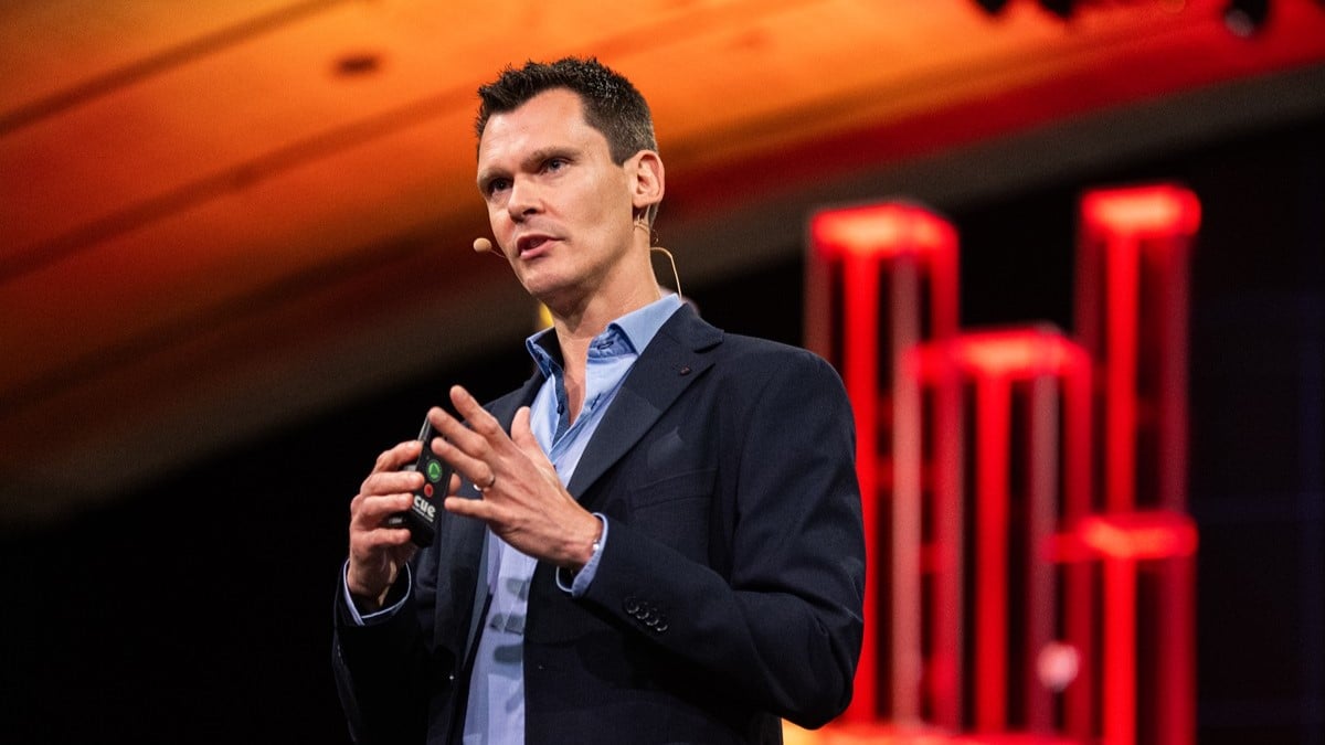
It’s not hard to find Arie den Boef in the loud lunchtime flurry of a pre-coronavirus ASML Plaza in Veldhoven for a chat about his latest work. He is a beacon of serenity. The fellow's humility and curiosity make him a favored and well-respected leader in ASML's global research community. At ASML, fellows are chosen for their pioneering work in service of the company and the industry, and over the years, many young engineers have sought Arie's mentorship and inventive mind for guidance.
"As a fellow in the field of metrology, I am in a unique position to give back,” says Arie. “I can help colleagues and PhD candidates to sharpen their thinking, to set them on new and interesting paths. And I can help the company chart its course into the future."
But to understand that future, we must begin in the past.
The metrology spark
Arie began his career as a research assistant at the renowned Philips Research physics labs, where a crucial part of the innovation mindset was to trust in creative freedom, self-starting and mentoring. “Later, when I joined ASML in the late 90s as a system engineer, I felt that same spark. After a few years I joined ASML’s Research team, which has the broadest view on the company’s technology development. It was the perfect environment to start fleshing out my ideas on optical metrology.”

“It was the perfect environment to start fleshing out my ideas on optical metrology.”
In the early 2000s, metrology wasn’t exactly new. Chipmakers had already been using optical systems to verify the quality of chip features on printed wafers for many years. But the penalty of getting a good look at a silicon wafer was steep: wafers could only be microscopically inspected by interrupting them from their automated flow through the fab. Moreover, the margins for error were getting smaller with every new chip generation, while the complexity and number of interconnected layers in the chip were increasing. Finding a problem with the layers on the chip early in the manufacturing process became a question of life or death: if metrology detected a problem early on, it could be corrected in the lithography machine. If metrology didn't detect the problem, the wafer would typically end up getting scrapped. And in the worst-case scenario, a problematic chip design moved into production, where it would be repeated again and again.
Arie saw that chipmakers needed a new approach to do measurements on chip structures and layers. They needed a system that would be able to do those measurements quickly, accurately and then loop the data back to ASML’s lithography system for real-time corrections to the manufacturing process. Arie’s first thought was to build a system that measured critical dimension uniformity (how well the smallest features on a chip were printed), but after talking to ASML’s customers, Arie concluded that the chipmakers’ struggle with overlay (how well the many different layers of a chip lined up) was actually the perfect challenge. His new metrology concept would be based on scatterometry.
Pioneering YieldStar
Arie’s scatterometry concept was deceptively simple: use a stack of target gratings within the different layers of the chip. By shining a light source on those gratings, advanced optics and a sensor could measure changes in the intensity of light coming back. If the target gratings didn’t line up within the specified error margins, the system would show a distortion in the inspection feed: bad overlay.
Painstakingly building a prototype metrology system by hand, he got the solid results that he was hoping for: measurements could indeed be carried out much faster without compromising accuracy. "Encouraged by my manager Jos Benschop [now ASML’s senior vice president of Technology], we pitched the research project to our chief technology officer Martin van den Brink. He also saw the potential of this technology for our customers. So, within months, dozens of engineers were working together to bring this new machine to life. We dubbed it ‘YieldStar’. Within a few years, it had become a crucial product in ASML’s holistic lithography portfolio."
YieldStar was a paradigm shift for ASML and our customers. The speed, accuracy and integration with ASML's lithography systems gave chipmakers the chance to tweak their production process without losing precious manufacturing time. Within a few years, YieldStar had become a crucial product in ASML's holistic lithography portfolio. Within a decade, we had an installed base of hundreds of YieldStar systems around the world and a packed innovation roadmap stretching well into the 2020s.

Within a few years, YieldStar had become a crucial product in ASML’s holistic lithography portfolio.
But as lithography systems continue to push the edge of technology in chip manufacturing, YieldStar's metrology performance has had to keep up.
In today's most advanced chip nodes, the requirements are so critical that any small measuring mistake might have a big impact on the customer's yield. And on top of that, chipmakers struggle with metrology challenges that are not always covered by YieldStar’s capabilities.
"YieldStar's most advanced optical sensor operates over a wavelength range of hundreds of nanometers. Ideally, you would broaden that range so the sensor can cover a larger application space and capture more information," Arie explains. "But there's a tricky trade-off with the optical design. More advanced optics would capture a limited set of wavelengths at much higher cost. Lower-tech optics could cover a much broader spectrum – but would produce imperfect images."
He decided to ask himself a fundamental question. "If I could start all over with YieldStar, knowing what I know now...how would I design a metrology system that tackles challenges cost-effectively at higher productivity and accuracy?”
Spoiler alert: complex optical designs wouldn't make the cut.
Computational imaging for metrology
In addition to his role as ASML Fellow, Arie is a part-time professor at the Vrije Universiteit in Amsterdam and the Research Center for Nanolithography (ARCNL). He heads a small group that does fundamental research in the field of computational imaging. "With the aid of computational imaging, it might be possible to achieve the quality of optical imaging that metrology will need—but instead of using an advanced and costly optical design, this technology would use only simple optical elements,” he says.
In conventional imaging, when light is bounced off an object, a lens bundles those scattering light rays and focuses them onto a sensor to show the image. More advanced optical elements and more sensitive sensors will create better images: just think of a professional camera with a set of lenses and top-notch sensor.
Computational imaging, on the other hand, uses raw computing power to get the image of an object. A simple optical design first generates an imperfect image. Advanced algorithms then analyze those imperfections. Finally, a heavy-duty computer determines the corrections that are needed and generates a sharp image.
Arie compares it to the camera on a modern smartphone. "What every smartphone manufacturer is trying to do is to put the imaging quality of a high-end camera in a tiny form factor, so without any protruding lenses. That means relying on algorithms to optimize the image for you." Computational imaging moves part of the complexity from advanced optics to smart algorithms.

Computational imaging moves part of the complexity from advanced optics to smart algorithms.
From research to realization
As far as his second paradigm shift goes, Arie and the team at ARCNL aim to bring their research concept to life over the next 3 to 4 years as a prototype metrology system. That means they don't just need to get the theory right as scientists – they need to be practical at the same time. “I am a researcher at an engineering company. It’s not a given that you can always bring those worlds together. If 30% of what we do in research makes it into an ASML product, I think we’re doing a fantastic job. And in this case, we’re aiming for an entirely new kind of metrology system.”
So, the bar is high. Arie’s colleagues in ASML’s Applications team (the part of the business responsible for metrology and inspection systems) are following the progress with serious interest. Arie: “The goal is to demonstrate a performance that would be impossible to achieve with classical optical design methods. The prototype’s capabilities would range from the visible part of the spectrum all the way to the infrared – with just a compact sensor, a single lens and optimized algorithms.” The team published a paper on their prototype setup in April 2020.
"I’m convinced that computational imaging offers a real opportunity for metrology, but I see this kind of research also having a wider impact on science, industry and society," Arie concludes. "With optics no longer being the limiting factor in imaging, you will see advances in camera- and sensor-based consumer products, medical technologies and industrial process monitoring. And thanks to smarter algorithms, the continuing rise of computing power in advanced chips and the fast progress in image sensors, computational imaging has a bright future."