ArF light source
Resolution
Projection optics
Wafers per hour
Key features & benefits
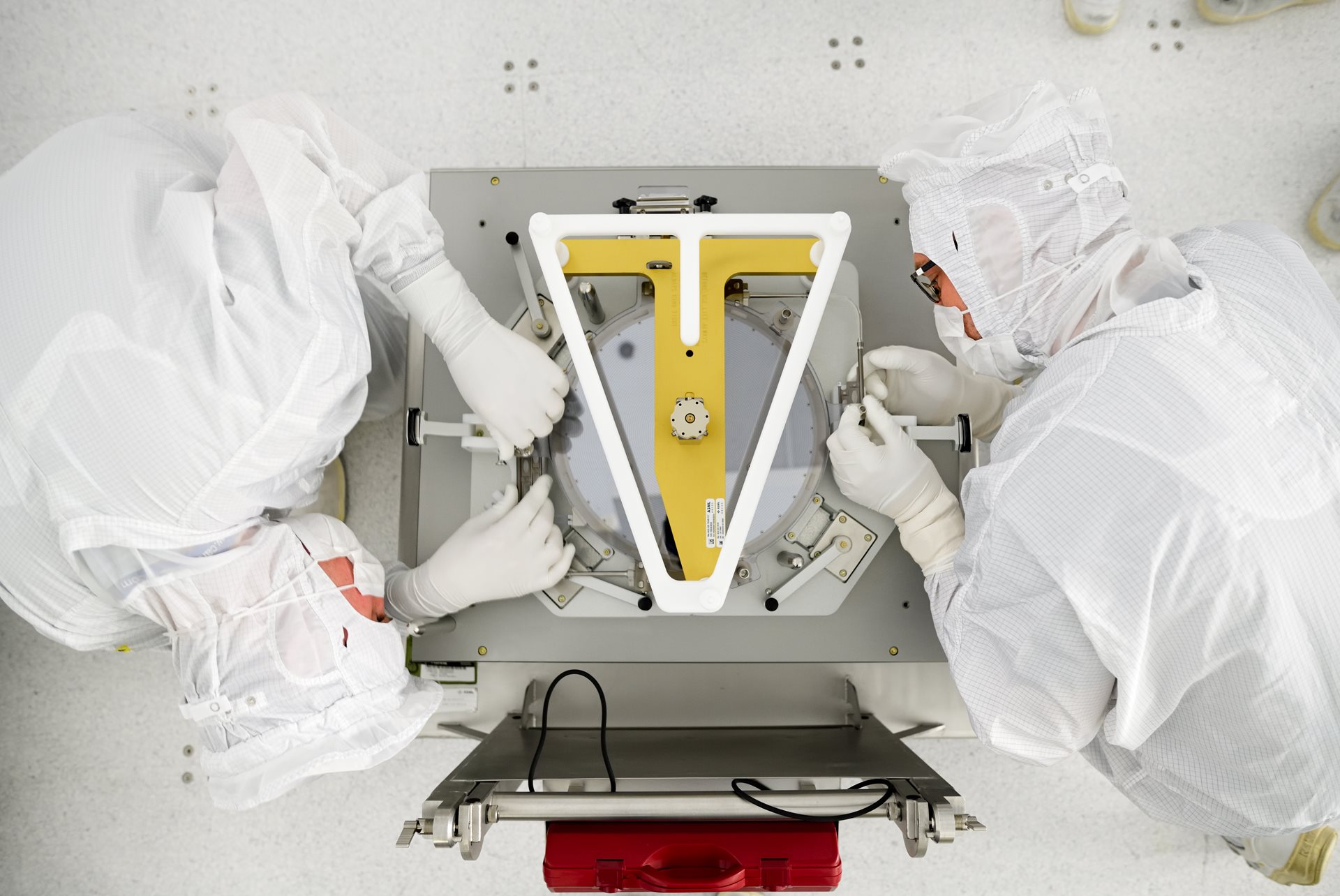
Like the TWINSCAN NXT:2000i, this step-and-scan system is a high-productivity, dual-stage immersion lithography tool designed for volume production of 300 mm wafers at advanced nodes.
By combining high productivity and excellent image resolution with unprecedented overlay and focus performance, the TWINSCAN NXT:1980Di addresses multiple patterning requirements and thus provides our customers with a cost-effective solution for advanced nodes.
01. Productivity
In this system, novel gas lifetime extensions reduce machine downtime and reinforce proven 6 kHz ArF laser technology to provide high power to support high throughput. Immersion hood design improvements widen the window to optimize defectivity using low contact angle resists without topcoat.
Together with the TWINSCAN NXT:1980Di maintenance scheduler, a comprehensive service package optimizes system availability by taking advantage of system idle time to perform required routine maintenance.
02. Optics
The TWINSCAN NXT:1980Di includes a 1.35 NA 193 nm catadioptric projection lens that can achieve production resolutions down to 40 nm (C-quad) and 38 nm (dipole) and an in-line design supporting full 26 x 33 mm field size, 4X reduction and reticle compatibility with existing designs.
Lens elements are equipped with manipulators to correct for optical aberrations, thus enabling maximum productivity for low-k1 applications. The FlexRay Prepared Illuminator allows maximum flexibility by extending the range of conventional and off-axis illumination to enable advanced pupil shaping for low-k1 imaging.
03. Imaging performance
The NXT:1980Di can achieve a ≤ 1.6 nm single-machine (dedicated chuck) full-wafer-coverage overlay, and a ≤ 2.5 nm matched-machine (to reference wafer) full-wafer-coverage overlay, thanks to improved wafer table flatness and wafer load grid, as well as improvements to the grid setup and layout-dependent grid calibration. These improvements also allow for better focus control.
The system’s Parallel ILIAS (PARIS) sensor allows customers to make parallel measurements of optical aberrations throughout the projection slit, which enables more accurate alignment, improved reticle heating correction and on-the-fly lens heating correction.
Finally, the SpotLess 2 Wafer Table Cleaning System automatically cleans excessive focus spots caused by particles on the exposure chuck without the intervention of an operator.