
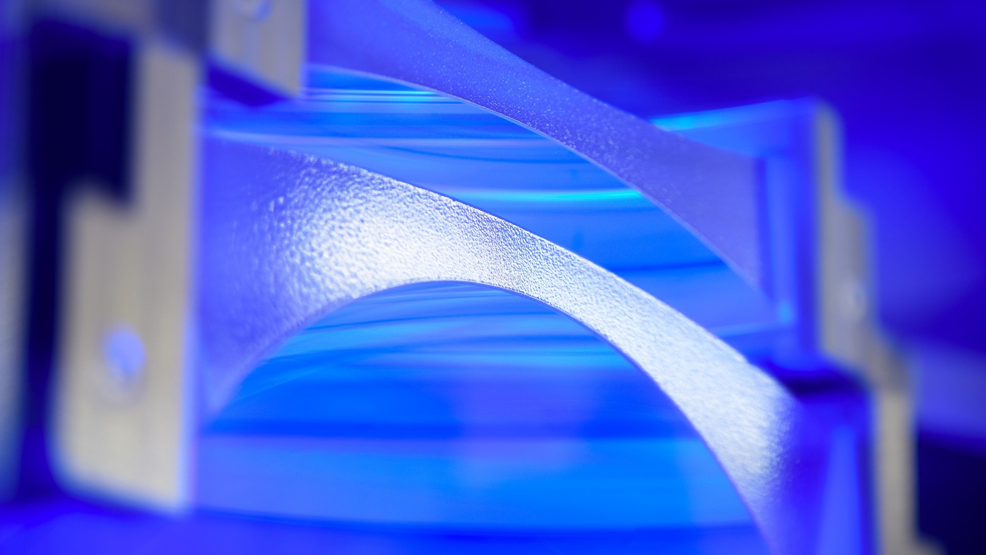
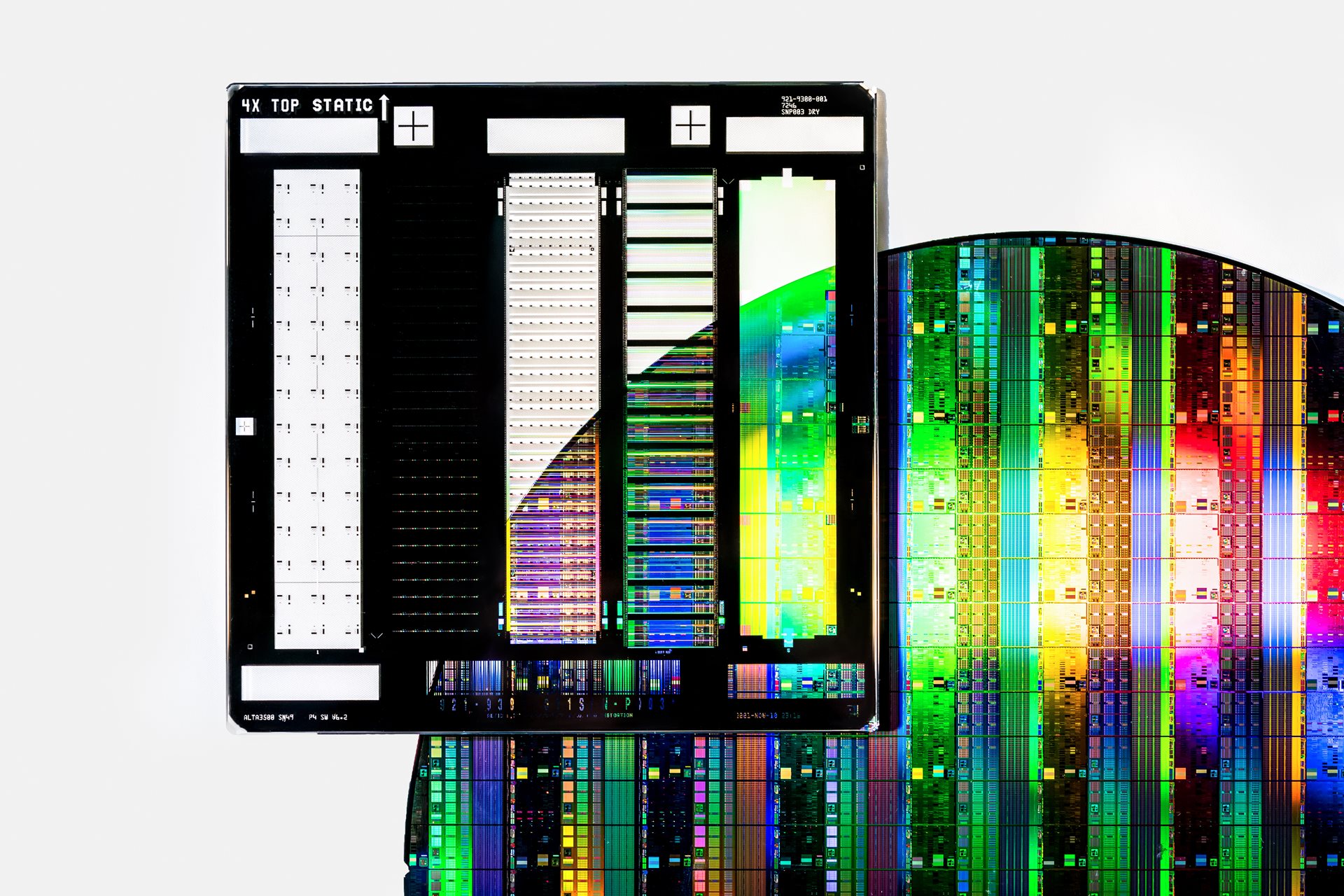
When we talk about a lithography machine’s optics, we aren’t talking about a single, simple lens. The core of every lithography machine is an extended optical system made up of dozens of individual components.
In deep ultraviolet (DUV) lithography systems, those components are lenses; in extreme ultraviolet (EUV) systems, they’re mirrors. Each component must be correctly positioned to within a nanometer to ensure image quality. ASML’s innovations in lens and mirror design have allowed chipmakers to reduce the sizes of features on microchips. Since the late 1980s, all our lithography systems have featured optics from our strategic partner ZEISS.
Numerical aperture
The smallest feature size that a lithography system can print is given by the Rayleigh criterion. According to the formula, one factor that affects how small the feature size can be is the numerical aperture (NA), which is a measure of how much light the system’s optics can collect and focus.
Increasing a system’s NA by using larger, higher-precision optics will shrink the size of the features it can print. With optical systems more than 1.2 meters tall and weighing more than a metric ton, our highest-resolution DUV lithography machines reach an NA of 1.35.
Our state-of-the-art EUV lithography machines, whose largest mirrors are 1 meter across and smooth down to tens of picometers, have an NA of 0.55. Although that’s lower than the NA in DUV machines, the EUV systems print smaller features because they use a much smaller wavelength of light – another factor in the Rayleigh criterion.
Immersion lithography
In 2003, ASML took an important step forward in improving the resolution of our DUV systems. We developed immersion lithography, which allows chipmakers to print even smaller features with the same wavelength of light by projecting the light through a layer of water between the lens and the wafer.
Without the water, reaching an NA of more than 1 was impossible. With it, our systems' optics reach an NA of 1.35.
Complexity brings control
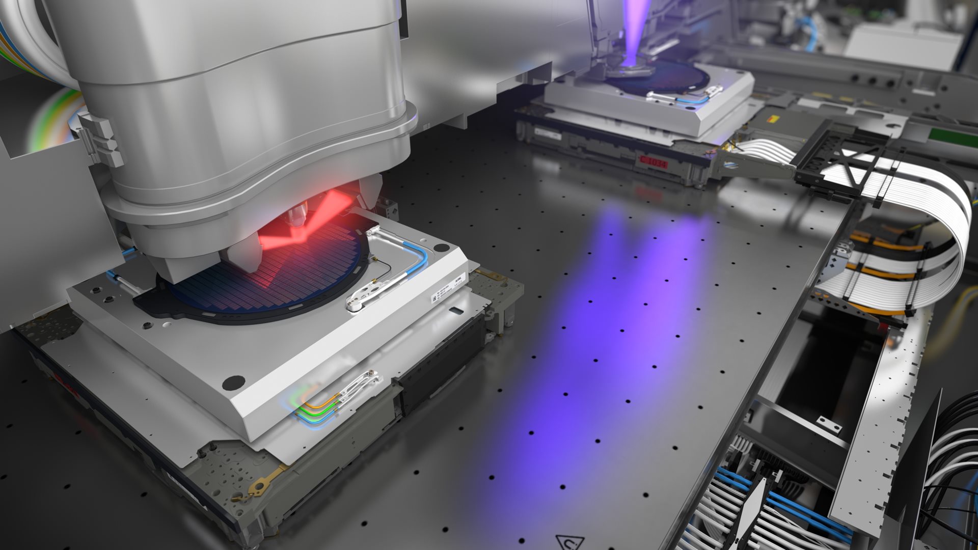
The sheer complexity of today’s lithography optics makes delivering high-quality optical systems a massive engineering challenge. But it also brings a unique opportunity to control every exposure with immense precision. Thousands of actuators allow the exact position and orientation of individual lens and mirror elements to be minutely adjusted to ensure the perfect image on the wafer every time.
Why are these adjustments needed? A working lithography system isn’t static. For example, the repeated intense light pulses used in lithography cause the optical system to warm up, which leads to distortions. These changes may be measured in millikelvins and nanometers, but that’s still enough to lead to defective microchips. Actuators in the optical elements actively compensate for these heating effects.

EUV needs mirrors
DUV lithography machines use lenses to focus light. But there are no lenses for EUV lithography. Since most materials absorb EUV light, the lenses would absorb the light in the system. Instead, we developed a brand-new optical system that uses ultrasmooth, multilayer mirrors inside a vacuum chamber. Each mirror has over 100 layers of materials that were carefully chosen and precisely engineered to maximize the reflection of EUV light.
Flatness is also crucial for EUV reflection. The mirrors are polished to a smoothness of less than one atom’s thickness. To put that in perspective, if the mirrors were the size of Germany, the tallest ‘mountain’ would be just 1 millimeter high.
High NA EUV
ASML’s latest EUV platform (EXE) increased the system’s NA from 0.33 to 0.55. Known as ‘High NA’, this platform has a novel optics design and significantly faster stages.
The High NA platform will enable geometric chip scaling beyond the next decade. It’s designed to enable multiple future nodes, starting at the 2 nm Logic node and followed by Memory nodes at a similar transistor density.

Lithography principles
The science behind the chip


More about ASML technology
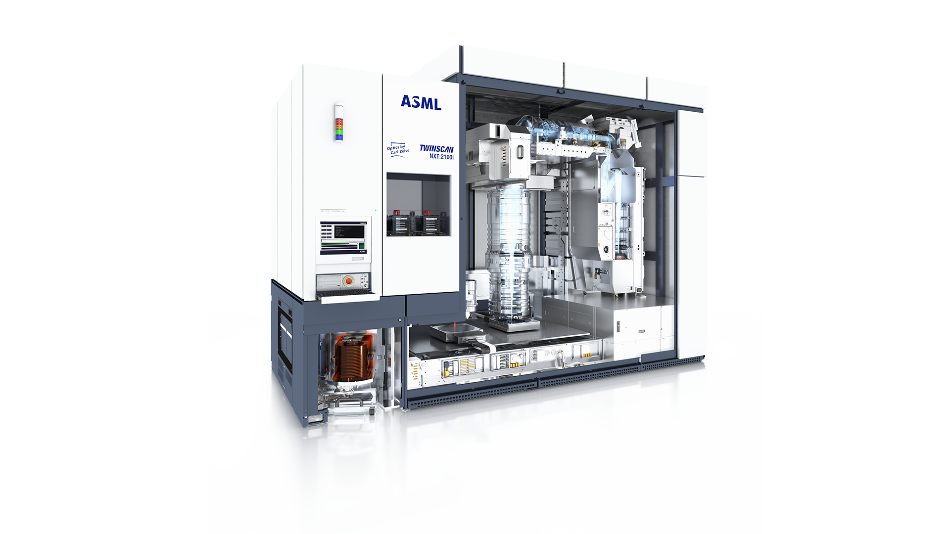
 EUV lithography systems
Providing highest resolution in high-volume manufacturing, ASML’s extreme ultraviolet lithography machines are pushing Moore’s Law forward.
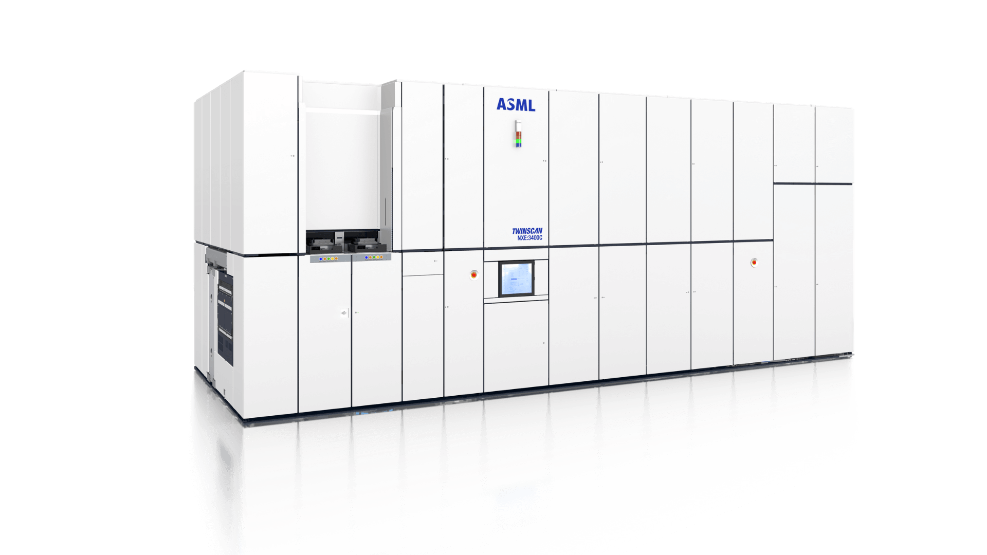
 DUV lithography systems
ASML's deep ultraviolet (DUV) lithography systems dive deep into the UV spectrum to print the tiny features that form the basis of the microchip.
 Metrology & inspection systems
Delivering speed and accuracy, our metrology and inspection portfolio covers every step manufacturing processes, from R&D to mass production.
 Computational lithography
ASML's industry-leading computational lithography products enable accurate lithography simulations that help to improve chip yield and quality.
Overachieving with overlay control
A new lens manipulator aligns microchip layers with unprecedented precision
