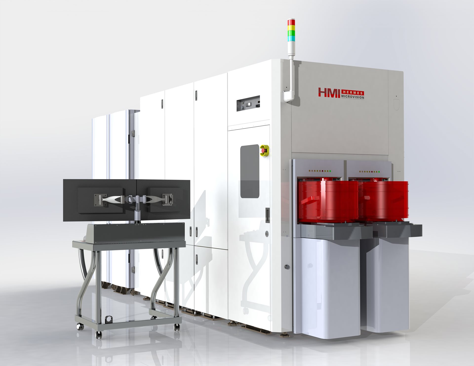
wafer inspection tool.")
Key features & benefits
As the world's first multiple e-beam (multibeam) wafer inspection tool, the eScan 1000 delivers a massive leap forward in high-resolution wafer inspection.
Targeting R&D for the 3 nm node, it is the first step in our multibeam roadmap to bring high-throughput, high-resolution e-beam inspection into volume manufacturing environments.
01. Throughput
The eScan 1000 is up to 600% faster than previous e-beam wafer inspection tools, thanks to its multibeam technology, high-speed wafer stages and advanced computational algorithms.
02. Multibeam technology
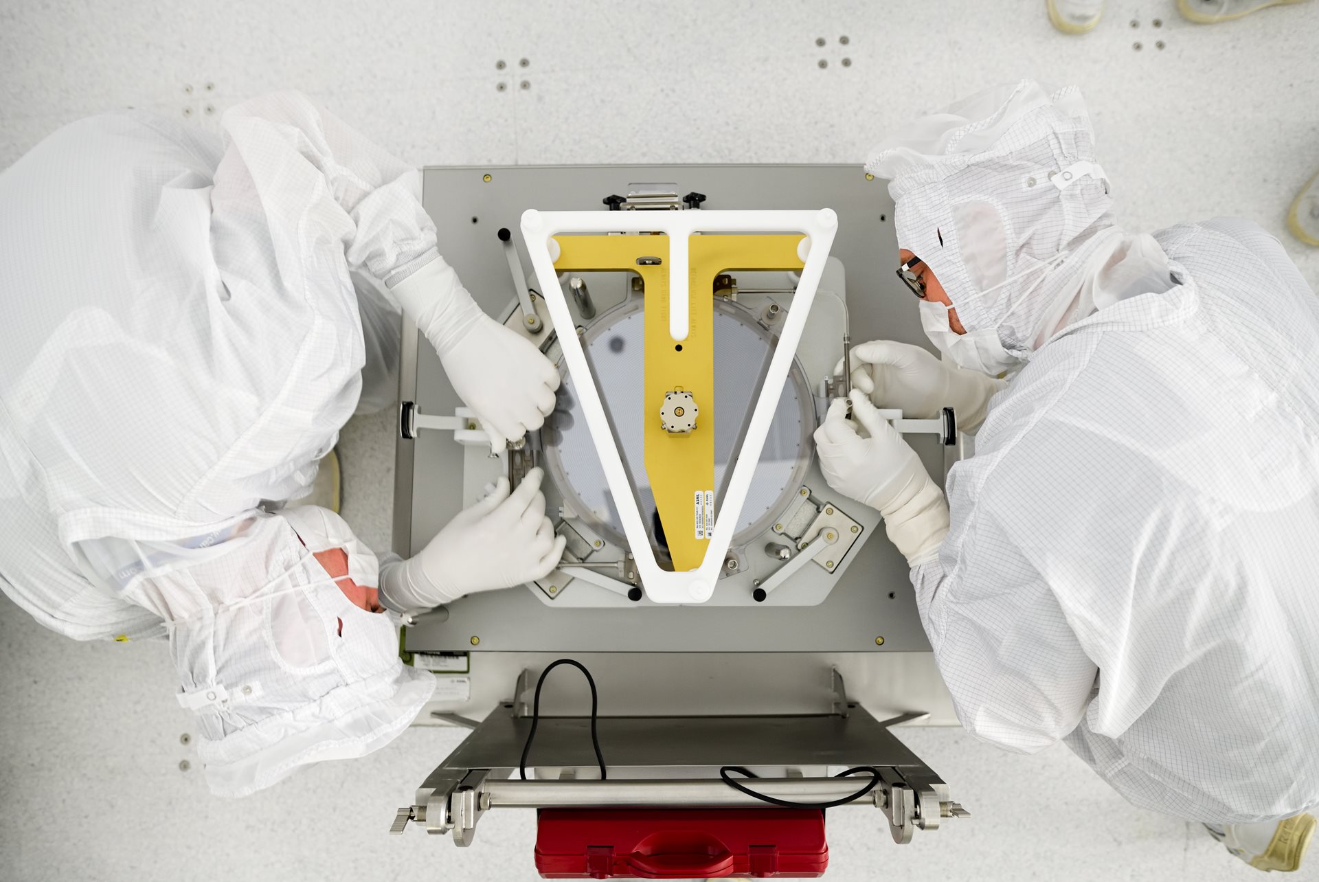
The eScan 1000 features nine electron beams in a 3x3 array enabling much faster scanning. Its single-source architecture ensures maximum flexibility in use while keeping crosstalk between beams to a minimum for more reliable results.
03. Multimode operation
The eScan 1000 can be used for both physical defect inspection and voltage contrast defect inspection. This allows it to detect electrical defects (including open, short and leakage defects) and patterning defects down to 10 nm.