ASML's history is rich with innovation and collaboration. Read more to learn how we've grown into the semiconductor industry leader we are today.
As they moved into their new quarters in a shed near the Philips buildings at Strijp T in Eindhoven, our founders could never have imagined that in just three decades, ASML would become a global innovation leader.
The 1980s: humble beginnings
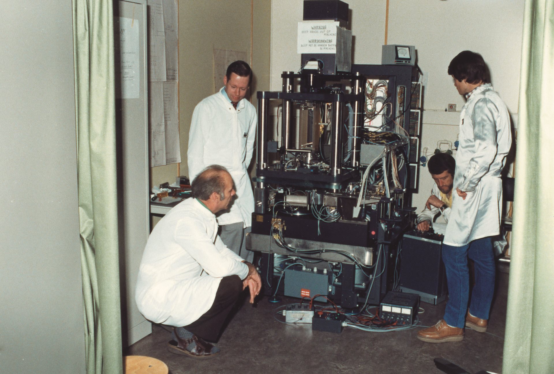
In 1984, electronics giant Philips and chip-machine manufacturer Advanced Semiconductor Materials International (ASMI) created a new company to develop lithography systems for the growing semiconductor market. Called ASM Lithography, we began our days inauspiciously, located in a leaky shed next to a Philips office in Eindhoven, the Netherlands. Building on the R&D that had been in the works since the early 1970s, that same year we launched our first system, the PAS 2000 stepper.
We grew fast, with Philips and ASMI scaling their investments to help make ASML a success. In 1985, with 100 employees on board, we moved into our newly built office and factory in Veldhoven, just a few kilometers from the Philips research labs. In 1986 we brought the PAS 2500 stepper to market, featuring new alignment technology that would be the foundation for many future innovations in our machines. That same year we established our existing partnership with lens manufacturer Carl Zeiss.
By 1988, we had begun to make in-roads in the Asian market, after Philips established a joint-venture foundry in Taiwan. In the United States, we grew from a few employees to 84, spread over five office locations. But in a market of fierce competition and many suppliers, the small unknown company from the Netherlands couldn’t catch a break. ASML had few customers and was unable to stand on its own two feet. Making matters worse, shareholder ASMI was unable to maintain the high levels of investment with little return and decided to withdraw, while the global electronics industry took a turn for the worse, and Philips announced a vast cost-cutting program. The life of our young cash-devouring lithography company hung in the balance. Guided by a strong belief in the ongoing R&D and in desperate need of funds, ASML executives reached out to Philips board member Henk Bodt, who persuaded his colleagues to lend a final helping hand.
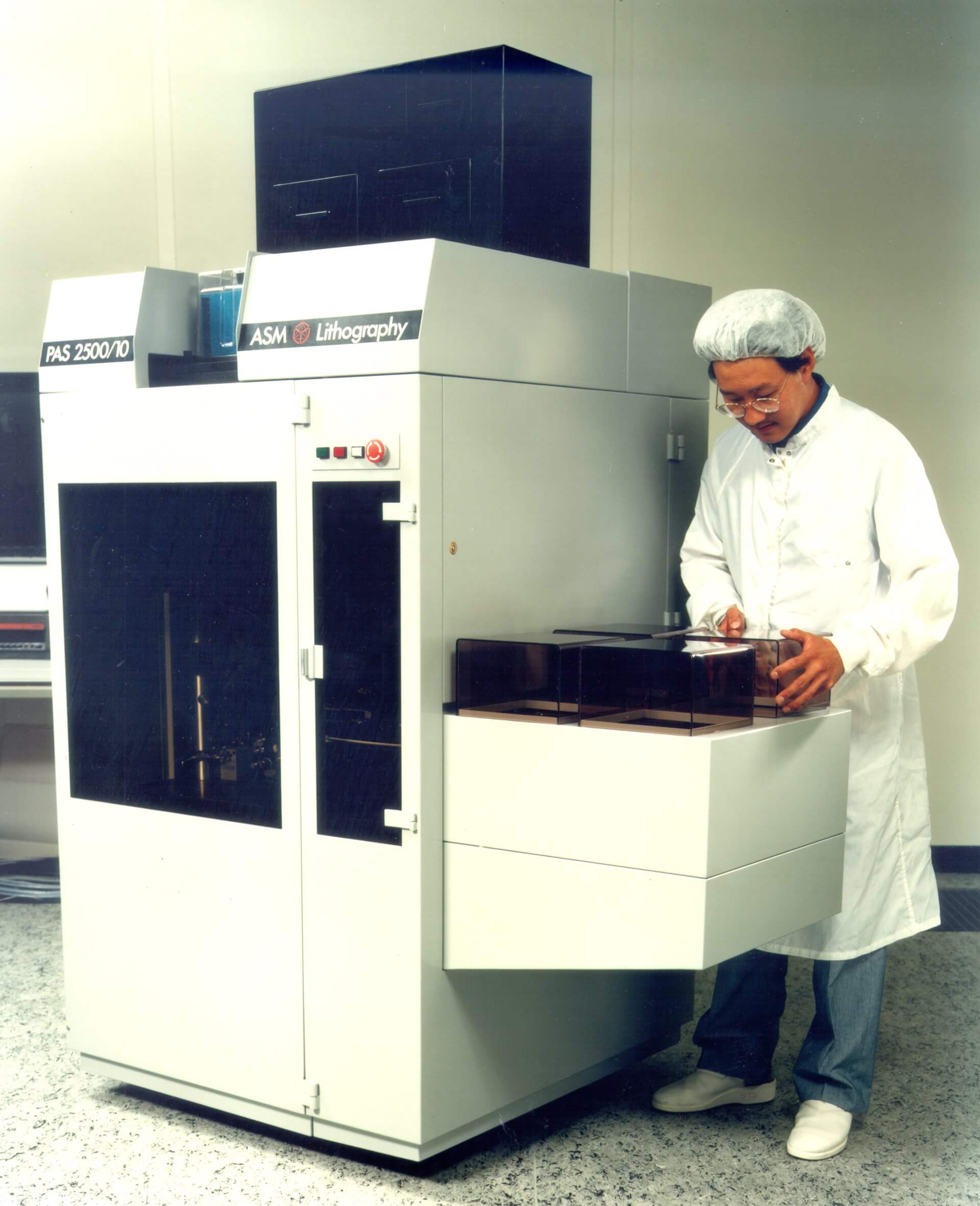
During this decade we launched what turned out to be our breakthrough platform, the PAS 5500. These classic lithography systems are still in use at customer fabs today.
The 1990s: from helping hand to IPO
The investment was put to good use. Within the year, we launched a breakthrough platform, the PAS 5500. With its industry-leading productivity and resolution, the PAS 5500 brought on board the key customers that ASML needed to turn a profit. It was a first step to maturity. In 1995, ASML became a fully independent public company, listed on the Amsterdam and New York stock exchanges. Philips sold half of its shares at the IPO and sold off the rest in the following years. The IPO brought in the capital to fuel our growth further, and we expanded our R&D and production facilities at De Run in Veldhoven, which would later become our new headquarters.
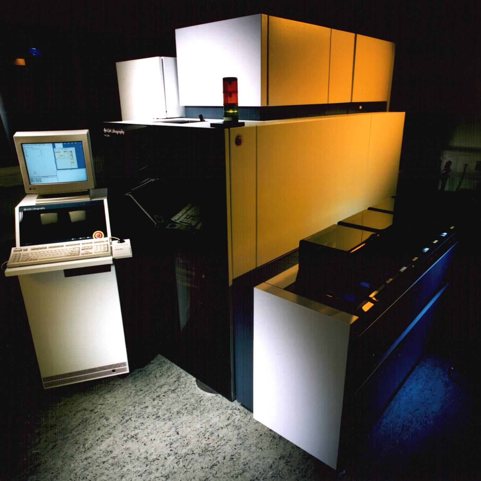
During the 2000s we drastically improved our systems' resolution, with immersion technology, and productivity, with our revolutionary dual-stage TWINSCAN technology.
The 2000s: TWINSCAN and immersion technology pave the way
In 2001, we introduced the TWINSCAN system and its revolutionary dual-stage technology. These systems expose one wafer while the next wafer is being measured and aligned, which maximizes the productivity and accuracy of the system, boosting ownership value for our customers. In the same year, we completed the acquisition of the Silicon Valley Group to further strengthen ASML’s capabilities in semiconductor technological advancement. The TWINSCAN AT:1150i debuted as the first immersion machine in 2003, followed by the TWINSCAN XT:1250i, XT:1400i, and in 2006 the first volume production machine for immersion, the XT:1700i. In 2007, we shipped the TWINSCAN XT:1900i immersion system with a numerical aperture of 1.35 – the highest in the industry. With this new technology, we enabled our customers to produce even smaller chip features by projecting light through a layer of water between the lens and the wafer.
Later in 2007, we acquired BRION, a leading provider of semiconductor design and manufacturing optimization solutions. This was the start of our ‘Holistic Lithography’ strategy. We united our knowledge of lithography systems with the skill to optimize the chip manufacturing process before, during, and after lithography. Another key product in the early phase of our Holistic Lithography strategy was YieldStar, our metrology system which provides real-time measurements and corrections during chip manufacturing. The first YieldStar (250D) was shipped to customers in 2008.

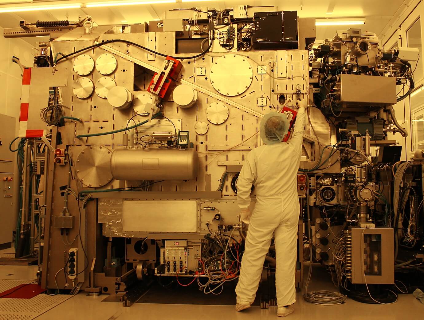
Starting in the 2010s, we again changed the face of the semiconductor industry by introducing EUV lithography.
The 2010s: the holistic era
In 2010, we shipped the first prototype extreme ultraviolet (EUV) lithography tool (TWINSCAN NXE:3100) to the research facility of an Asian chipmaker, marking the beginning of a new era in lithography. EUV lithography uses light of a shorter wavelength to manufacture smaller chip features, resulting in faster, more powerful chips.
In 2013, we acquired Cymer, the San Diego-based manufacturer of lithography light sources, to accelerate the development of EUV. We shipped the second generation EUV system (NXE:3300) that year, with the third generation EUV system (NXE:3350) following in 2015. EUV lithography turned the corner in 2016, when customers began ordering our first production-ready system NXE:3400 in batches. During this time, we continued to improve the performance of our immersion lithography systems, and the NXT1970Ci and NXT1980Di, the work horses of the chip industry, were installed in customer factories around the world. For more information, visit Cymer.
We expanded our holistic lithography portfolio in 2016 with the acquisition of Hermes Microvision (HMI) , a leading supplier of e-beam metrology tools. Our joint effort resulted in the first shipment of the e-beam pattern fidelity metrology system (ePfm5) in 2017.
Following the liquidation in 2018 of the high-tech company Mapper based in Delft, the Netherlands, ASML agreed to acquire the company’s intellectual property assets . We also offered suitable positions to Mapper’s highly skilled employees working in Research & Development and product assembly.

No one could have predicted the challenges that the world would face at the dawn of this decade. Yet our teams persevered, achieving several significant milestones against the odds.
The 2020s: unprecedented challenges, impressive innovations
At the beginning of 2020, EUV moved into high volume manufacturing and we celebrated the 100th EUV system shipment. But 2020 was also significant for another reason: the COVID-19 pandemic. Our teams around the world proved their ability to adapt and improvise by innovating new ways to support customers from a distance, lending their expertise to the pandemic response and reaching out to support our local communities.
In November 2020, the acquisition of Berliner Glas Group was completed and we officially welcomed the Berliner Glas team to the ASML family. The technical glass division of the group was divested to Glas Trösch Group in April 2021.
In 2023, we shipped the first of our next-generation EUV systems with a higher numerical aperture of 0.55 (known as ‘High NA’). This platform, called EXE, has a novel optics design and significantly faster stages.

