4-minute read - by Christine Middleton, January 25, 2024
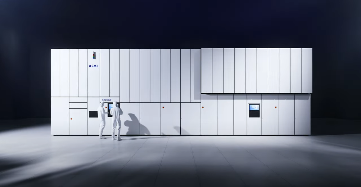
After a decade of R&D, ASML shipped the first modules of the first High NA EUV lithography system to Intel in December 2023. The TWINSCAN EXE:5000 represents a significant step forward for cutting-edge chip manufacturing.
Chipmakers rely on shrink – making transistors smaller and packing more of them onto silicon wafers – to drive advances in microchip technology. It’s not the only way to improve chips; novel architectures, for example, can also enhance performance. But there’s a reason why Moore’s Law is essentially the law of the land: Shrink has been behind an exponential growth in computing power for more than 50 years.
For years we’ve been pushing deep ultraviolet (DUV) lithography to its limits. To reduce the size of the smallest feature that can be printed, known as the critical dimension (CD), there are two main knobs we can turn: the wavelength of light, λ, and the numerical aperture, NA. Now, however, there’s little room left to adjust those knobs in our DUV systems.
EUV lithography allowed us to make a big turn of the wavelength knob: It uses 13.5 nm light, compared to 193 nm for the highest-resolution DUV systems. When our first pre-production EUV lithography platform, the NXE, first shipped in 2010, it delivered a drop in CD from more than 30 nm in DUV down to 13 nm with EUV.

What is High NA EUV lithography?
High NA EUV is the next step in our constant pursuit of shrink. Like NXE systems, it uses EUV light to print tiny features on silicon wafers. And by turning the NA knob, we deliver even better resolution: The new platform, known as EXE, offers chipmakers a CD of 8 nm. That means they can print transistors 1.7 times smaller – and therefore achieve transistor densities 2.9 times higher – than they can with NXE systems.
How did we get a higher resolution in our High NA EUV systems? Why are chipmakers investing in the new technology? And what does this mean for you? Read on to learn more.
1. Larger, anamorphic optics for sharper imaging
The headline advance in High NA EUV lithography is the new optics. The ‘NA’ in the name refers to numerical aperture – a measure of the ability of an optical system to collect and focus light. And it’s called High NA EUV because we’ve increased the NA from 0.33 in our NXE systems to 0.55 in EXE systems. The higher NA is what gives the systems their better resolution.
Implementing this increase in NA meant using bigger mirrors. But the bigger mirrors increase the angle at which light hit the reticle, which has the pattern to be printed. At the larger angle the reticle loses its reflectivity, so the pattern can’t be transferred to the wafer. This issue could have been addressed by shrinking the pattern by 8x rather than the 4x used in NXE systems, but that would have required chipmakers to switch to larger reticles.
Instead, the EXE uses an ingenious design: anamorphic optics. Rather than uniformly shrinking the pattern being printed, the system’s mirrors demagnify it by 4x in one direction and 8x in the other. That solution reduced the angle at which the light hit the reticle and avoided the reflection issue. Importantly, it also minimized the new technology’s impact on the semiconductor ecosystem by allowing chipmakers to continue using traditionally sized reticles.
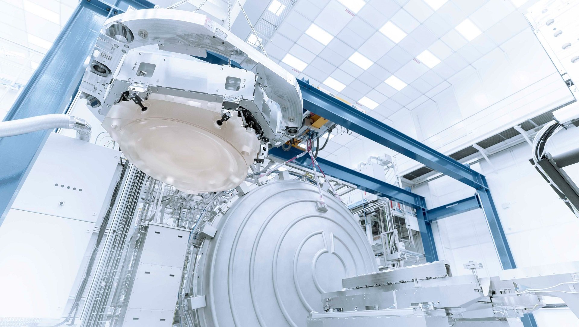
Fly through a High NA EUV lithography system
2. Faster stages for higher productivity
Because of their anamorphic optics, EXE systems have exposure fields half the size of their NXE predecessors. It therefore takes twice as many exposures to pattern a single wafer.
Twice as many exposures could have meant twice as long to print a wafer. Instead, we took it as a challenge. The solution? Much faster wafer and reticle stages. The wafer stage in an EXE system accelerates at 8g, twice as fast as the NXE’s wafer stage. And the EXE’s reticle stage accelerates four times faster than the NXE’s – 32g, the equivalent of a race car going from 0 to 100 km/h in 0.09 seconds.
With its new stages, the TWINSCAN EXE:5000 can print more than 185 wafers per hour, an increase compared to the NXE systems already being used in high-volume manufacturing. And we have a roadmap for increasing that to 220 wafers per hour in 2025. This productivity was key to making sure the integration of High NA into chip fabs was economically viable for chipmakers.
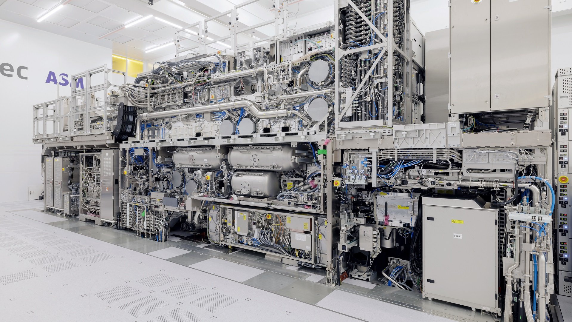
High NA EUV mirror testing at ZEISS (Credit: ZEISS SMT)
3. Simpler manufacturing for cost efficiency
High NA EUV lithography will enable chipmakers to print the smallest features on the most advanced microchips. But in the meantime, chipmakers haven’t just been waiting around. They’ve found other ways to get around the resolution limitations of their lithography systems by using more complicated production processes.
These workarounds come at a cost. They increase production time and provide additional opportunities to introduce defects that could affect the chip’s performance. With its CD of 8 nm, the EXE:5000 enables chipmakers to simplify their manufacturing processes. The result? More cost-efficient production of advanced microchips.
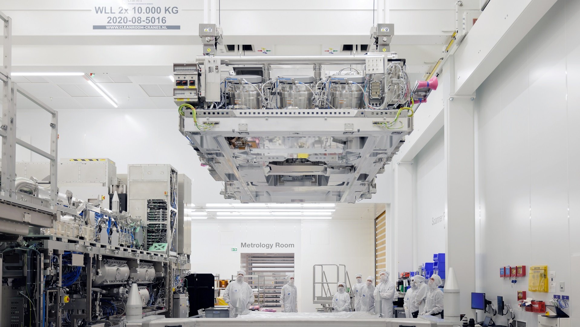
An open, fully assembled TWINSCAN EXE:5000
4. Commonality and modularity for better performance
The EXE:5000 represents an evolution of EUV lithography, not a revolution. We’ve reused as much of our existing EUV technology as possible and changed only those aspects necessary to deliver the system’s resolution and productivity enhancements. And, like our NXE EUV systems, EXE systems are made up of modules that can be independently tested before being integrated into a complete system.
Why did we prioritize commonality and modularity throughout our EUV lithography systems? Because that way all of our systems benefit from lessons learned over 20 years of EUV development. Using tried-and-tested technology reduces the risk of things going wrong. And the modules streamline the system’s installation and integration into a customer fab. That means the systems will start producing chips more quickly – our customers will start their R&D in 2024–2025 and move into high-volume manufacturing in 2025–2026.
The quick timeline is good news for everyone: The sooner these systems start printing state-of-the-art chips, the sooner the cutting-edge technology they enable will be available.
5. Improved chip functionality, performance and energy efficiency
The 8 nm resolution of the EXE:5000 means that chipmakers can pack more transistors into a single chip. Smaller transistors are more energy efficient – that means the chips will be able to do more with less. So the tiny features printed by the EXE:5000 will form the foundation of the most advanced microchips. And, because of the system’s productivity, chipmakers can manufacture these chips in huge numbers.

The impact of High NA EUV lithography
Chip innovation is increasingly important in today’s digital world. Consumers expect new types and generations of electronic devices that are smaller but do more, and do it better and faster. With High NA EUV lithography, chipmakers can deliver on those consumer demands.
The first chips made using the EXE:5000 will be 2 nm node Logic chips. Memory chips at a similar transistor density will follow. These chips will combine the tiniest features with leading-edge architectures to power the technology of the future: robotics, artificial intelligence, the internet of things, and beyond.
To learn more about our EUV lithography systems, how EUV works and the road to EUV, check out our EUV lithography systems page.