History of HMI
The company – formerly called Hermes Microvision, Inc. – launched its R&D operations in Silicon Valley, gathering some of the brightest minds in physics, electron optics, image processing, software, electronics and control, and mechanical structure to address the semiconductor industry’s growing challenges with shrinking microchips.
Read more about HMI's history
The first e-beam inspection system
HMI’s first e-beam inspection system, eScan300, was developed in 2003, marking the company’s first step towards improving the performance of microchip manufacturing.
Following the company’s creed to “solve customers’ problems, become the customers’ partner, and build up mutual trust with customers,” HMI became a leader in wafer defect inspection technology. HMI’s dedication to the R&D, manufacturing, sales and service of its products continues today as part of ASML.
HMI product portfolio
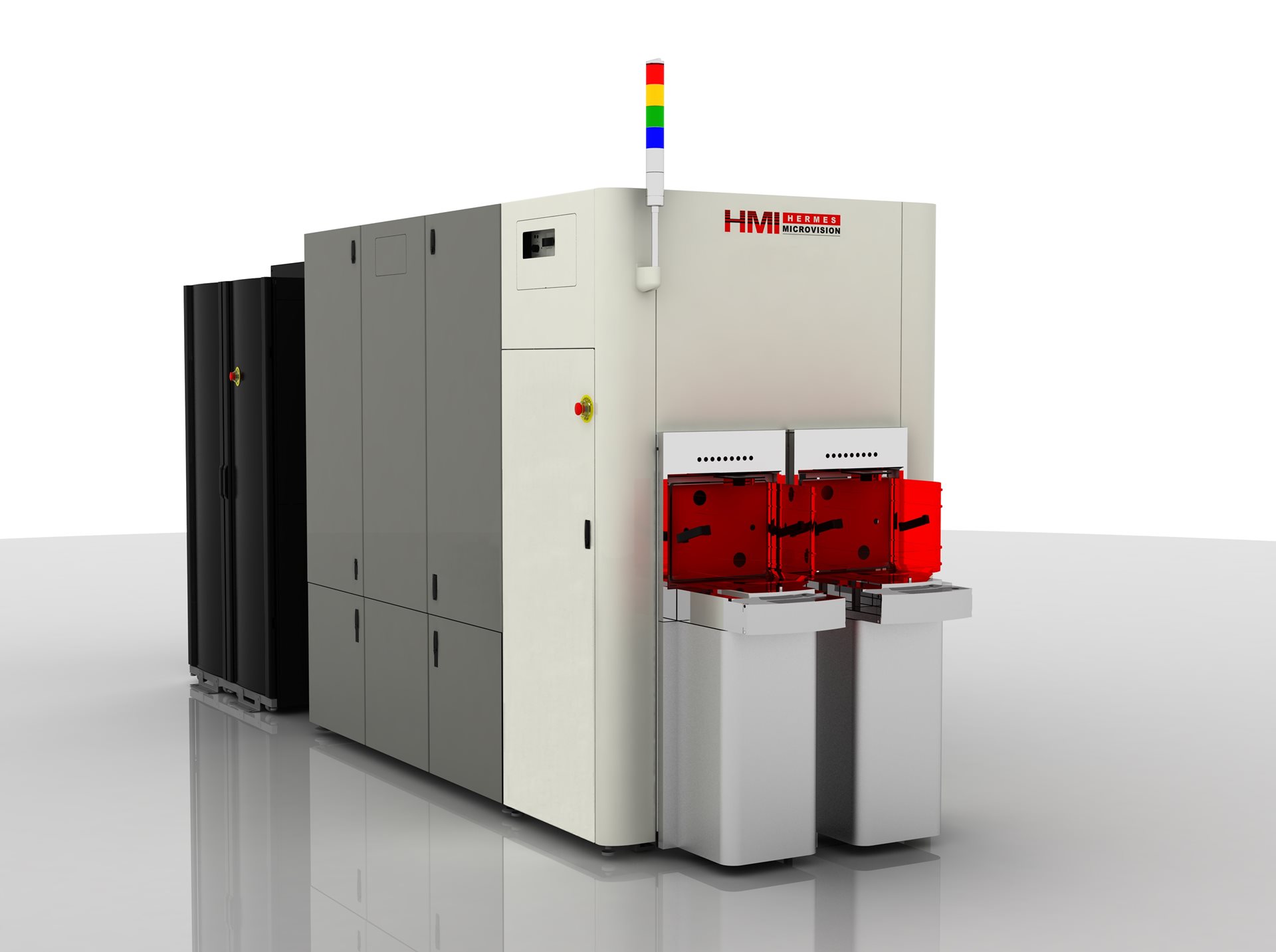 HMI eScan 430
Fast e-beam inspection for process development and production monitoring for 3D NAND and other advanced chips.
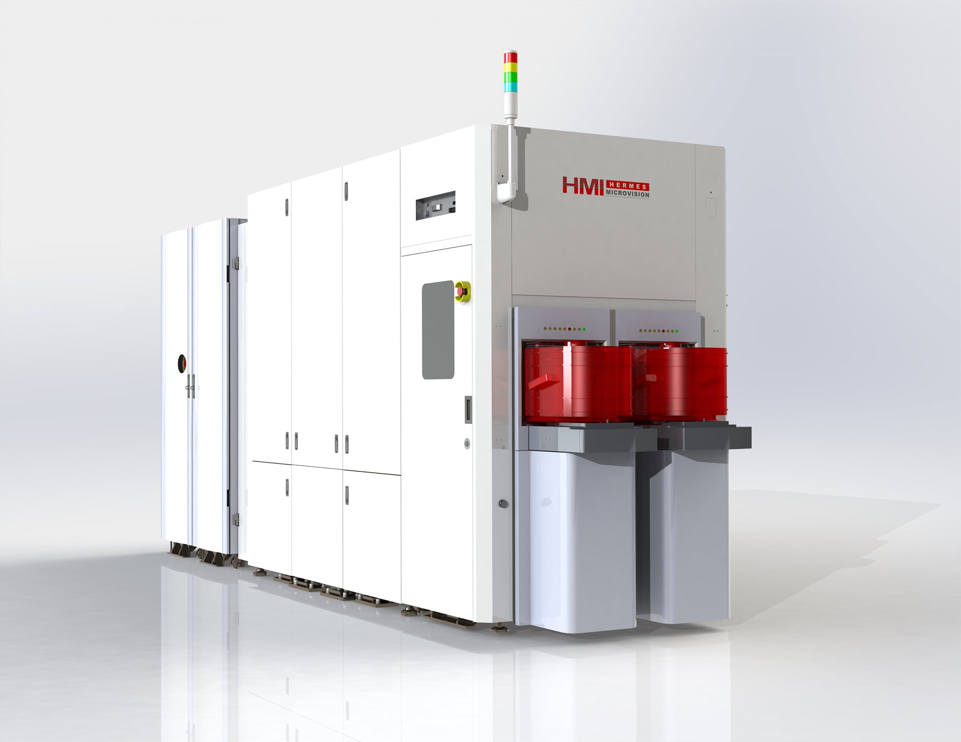 HMI eScan 600
Flexible e-beam inspection solution detects multiple defect types in one system.
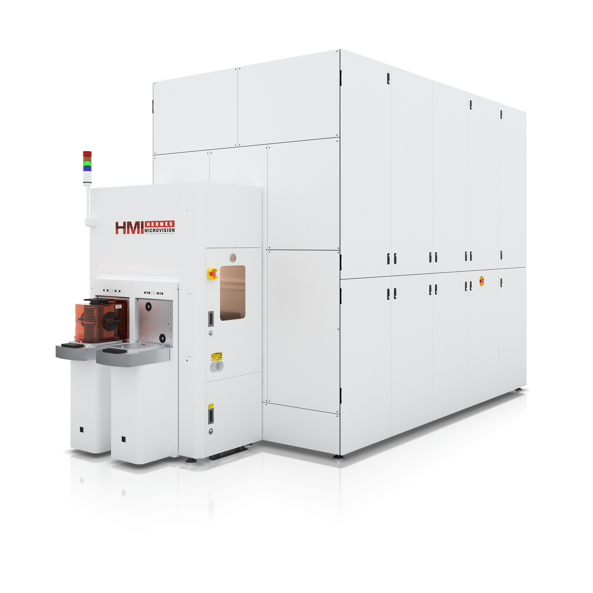 HMI eScan 1000
The world’s first multiple e-beam (multibeam) wafer inspection tool.
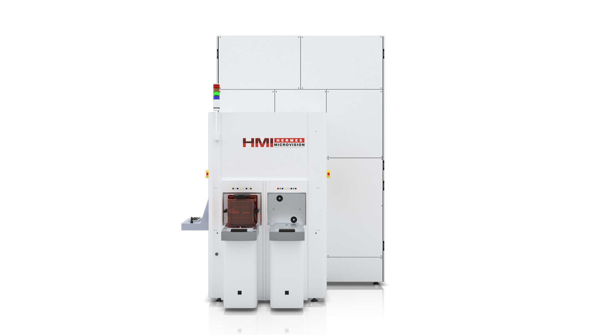 HMI eScan 1100
The first generation multiple e-beam (multibeam) wafer inspection tool for in-line defect inspection applications.