Our business strategy

ASML's strategy is built on six priorities, through which we keep powering technology forward.
Select a priority below to learn more, or continue reading for the full stories.         

1. Deepen customer trust

Consistently deliver innovative, high-quality and reliable holistic lithography solutions that foster long-term customer partnerships and set industry standards for excellence
Keeping our lithography systems running 24/7

At ASML, customer trust is a guiding principle woven into the daily work of engineers like Edison Alameda. As a second-line customer support engineer for EUV in Chandler, Arizona, Edison’s job is to ensure the smooth operation of some of the world’s most advanced semiconductor manufacturing equipment and serve as a bridge to the customers who depend on them.

ASML technician working on a machine component

Powering technology forward through customer collaboration

Read more


Prioritizing problems and executing solutions

Edison’s day starts early at 7:00. His first task is to review the pass-down report – a detailed summary of customer problems and the actions taken in the last 12 hours. Because customer support is a 24/7 operation, the night team ‘pass down’ their responsibilities to ensure continuity of service. Edison collaborates closely with first-line engineers, identifying the highest-priority issues and allocating tasks to ensure each challenge is handled quickly by the people with the right skillset.


By 8:00, Edison is preparing for a customer meeting to provide a status update and discuss upcoming focus and priorities. Edison presents his data analysis, supported by slides that outline the problem, the plan and the expected outcomes. Transparency is crucial. “We explain how we’re attacking the issue at hand, and how we’re going to move forward,” says Edison. “This reinforces the customer’s confidence in the team and the process.”


When a system is down, emotions can run high – and the pressure from the customer is palpable. First-line engineers are on-site for the task, while Edison reviews data traces remotely and coordinates the actions to solve the problem. His methodical, data-driven approach allows him to communicate clearly with the customer, requesting additional access time to the machine only when he can justify the need. Openness paired with evidence-based reasoning is critical in maintaining the customer’s trust, especially under stress.


If the problem can’t be solved by the first-line team, second-line generalists and competency engineering step in. These engineers have expertise in one or more modules of the systems. In the case of Edison, his competency is in positioning, which includes the wafer table, wafer stage and reticle stage.


Remarkably, about 95% of issues are resolved locally. “This really speaks volumes – in the way we organize, plan and build our action plans and solutions,” Edison points out. When local capacity reaches its limits or there’s a gap in the necessary skills, Edison taps into ASML’s regional customer support network.


In addition to managing escalations, Edison is also responsible for scheduled equipment maintenance. Lithography system downtime is very costly for customers because it can reduce fab output. Therefore, maintenance needs to be meticulously planned, reviewed and coordinated to help support maximum uptime. As part of this effort, he uses predictive analytics and dashboards to continuously monitor equipment health, allowing him to anticipate potential problems and maintain peak system performance.

Portrait of Edison Alameda, Customer Support Engineer

Edison Alameda, Customer Support Engineer


Customer advocacy and continuous learning

Edison sees himself as an advocate for the customers who use our systems and explains, “When a problem arises, I build a case using necessary data, respecting the sensitive nature of their information. This balance of openness and discretion is essential for maintaining trust in our relationship.”


Beyond problem-solving, together with his fellow second-line team members, Edison is continuously learning to keep himself at the forefront of evolving technology – through weekly knowledge-sharing, extensive knowledge transfer libraries and peers across the globe in Taiwan, South Korea or Europe, who all share and contribute to our knowledge base.


Ending on a high note

A successful day means the customer’s problem is solved or progressing toward resolution. For Edison, the most rewarding part of his job is successfully bringing the system back up and running, and earning the customer’s recognition and trust. He feels great pride in his personal contributions and the collective achievements of the team, knowing their efforts deliver real value to our customers. 

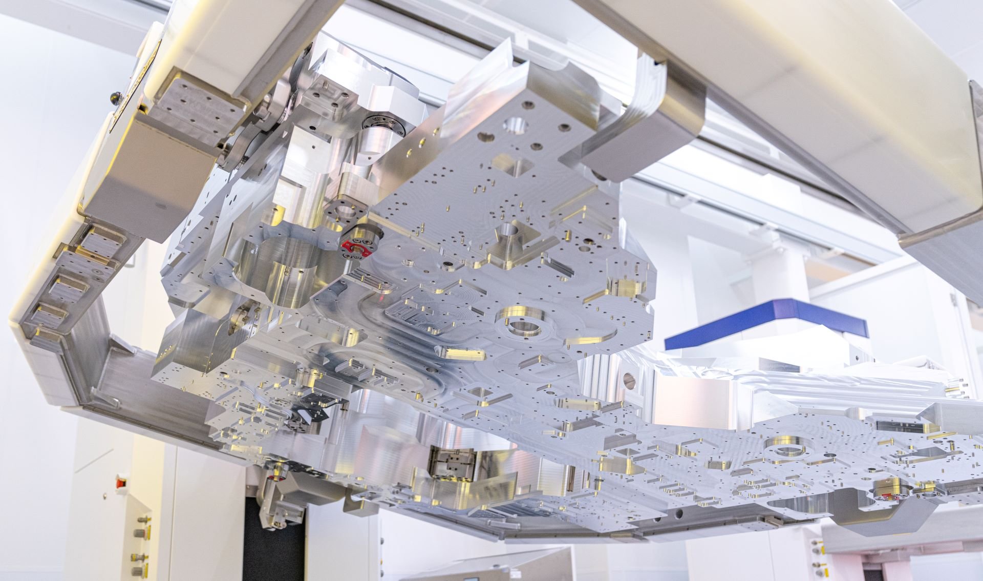
2. Extend our technology and holistic product leadership

Integrate hardware, software and emerging solutions to create industry-defining products for our stakeholders
1,000-watt EUV light source power shows path to higher productivity 

In April 2025, ASML reached a historic milestone: demonstrating the first ever 1,000-watt light source for EUV lithography. This breakthrough, built on 25 years of engineering advancements, showcases our ability to turn fundamental physics into scalable innovation that supports our customers’ roadmaps. It is a critical step toward faster, more cost-efficient production of tomorrow’s cutting-edge microchips that drive high‑performance computing and AI, while supporting innovation across industries like medical imaging, renewable energy, agriculture and modern consumer technology.

ASML technicians examining a machine part in a cleanroom

Powering technology forward through cutting-edge physics

Read more


Extreme ultraviolet (EUV) lithography, which uses 13.5 nanometer light, enables the production of the most advanced semiconductor features and plays a critical role in the high-volume manufacturing of today’s leading-edge microchips. However, such light can’t be produced by lamps or even directly by lasers. When ASML started developing EUV lithography about 25 years ago, it became clear that a completely new type of light source was needed.


EUV source

After looking at the alternatives, we chose an architecture based on laser-produced plasma (LPP), which promised a final source that required less downtime for maintenance and offered scalability to higher powers. With LPP, powerful laser pulses are fired at tiny droplets of tin travelling through a (near) vacuum – transforming the droplets into exploding balls of plasma 40 times hotter than the surface of the sun and causing them to emit an intense burst of EUV light.


To create enough EUV light for making microchips, this process is repeated thousands of times per second – 60,000 times per second in our latest commercial sources. The light is collected and channeled into the lithography system’s optics – no small feat, given that EUV light is absorbed by almost all materials. We worked closely with our optical partner ZEISS to develop a system using mirrors made up of more than 100 layers of precision-engineered materials.


Evolving to meet customers production needs

The source in our first prototype EUV lithography system, released in 2010, delivered just one watt of EUV light power – sufficient for customers to begin exploring EUV, but it fell short of the requirements for volume production. 


Reflecting on the early days, Jayson Stewart, now Head of Source Research, recalls: “For a long time, the output wasn’t powerful enough to make EUV a viable investment for customers. But those early wafers that were exposed – albeit very slowly – showed the potential, and we knew EUV lithography could be a key enabler for the industry.”


Creating a powerful and reliable EUV light source is both a physics challenge and an engineering one. We worked with our technology partners to push the forefront of science to improve the plasma explosions and found that flattening the tin droplet before triggering the explosion increased the EUV light output. We also developed a way to prevent feedback between the plasma and laser, enabling more powerful, stable laser pulses.

Portait of Jayson Stewart, Head of Source Research

Jayson Stewart, Head of Source Research


Many doubted we could ever deliver an industrial EUV source. The challenge was immense, but through insights like these, we pushed up the source output power step by step. 10 watts. 50 watts. 100 watts. In 2018, we reached 250 watts – enough for manufacturers to start volume production at 125 wafers per hour.


We continued to push for higher EUV power because faster systems help our customers operate more efficiently. By 2022, we had a prototype source delivering 500 watts.


Breaking the 1,000-watt barrier

Still, our customers' demand for EUV throughput was not slowing down. And neither was our innovation to deliver it. We set ourselves a new target: 1,000 watts.


A tremendous amount of work went into realizing that target, including the development of new plasma recipes and boosting the laser’s power. Our biggest leap forward was increasing the repeat rate – the frequency of exploding droplets – from 60 kHz to 100 kHz. That’s 100,000 droplets and plasma explosions per second! This helped to raise output power while increasing the power efficiency of the entire system. 


The long-awaited 1,000-watt milestone was finally achieved in April 2025 in a successful demonstration. Jayson highlights its significance: “Although we believe it will be some time before a commercial 1,000-watt source is ready, this demo clearly validates our approach, which can be scaled to even higher power levels. When our customers’ roadmaps require more EUV light to boost productivity, we’ll be ready.”

3. Strengthen ecosystem relationships

Collaborate with suppliers, academic partners and industry leaders to foster innovation, resilience and shared success across the value chain        
Getting even closer to our suppliers 

In the dynamic landscape of semiconductor manufacturing, ASML’s supply chain serves as the foundation of our operations, enabling us to push the boundaries of technology while meeting the evolving demands of our customers. With approximately 80% of our bill of materials sourced from a global network of suppliers, close collaboration and joint innovation have always been at the heart of our strategy. We believe this partnership model not only supports the reliability and quality of our products but also fosters a shared commitment to advancing Moore’s Law, which remains essential for the industry’s continued progress. Wayne Allan, EVP and Chief Strategic Sourcing & Procurement Officer, explains how his organization is strengthening ASML’s ecosystem relationships.

ASML equipment being lifted by a crane at an industrial site

Powering technology forward through collective innovation

Read more


What steps has ASML taken to deepen collaboration with suppliers?

Building on a foundation of collaboration over the past years, we’ve made significant strides in strengthening our supplier relationships, particularly near our global headquarters in Europe, where our robust network continues to play a pivotal role.


Our headquarters in Veldhoven, the Netherlands, serves as a hub for development, engineering and manufacturing – supporting seamless integration with suppliers on cutting-edge products and technologies that are in ongoing development. This proximity supports real-time collaboration, accelerated innovation cycles and efficient roll-out of new advancements. 


By working hand in hand with our partners, we’ve enhanced our ability to co-develop solutions that address complex challenges in lithography and metrology, maintaining our leadership in high-precision systems. 


What strategies are you implementing to evolve your supply chain and adapt to the diverse needs of global markets?

Looking ahead, we’re committed to evolving our supply chain to support sustainable growth and operational resilience. We’re actively expanding our sourcing footprint to include strategies that promote local repair and reuse, as well as localized sourcing for service operations where it makes strategic sense. This approach can reduce downtime for our customers while also contributing to environmental sustainability by minimizing waste and transportation impacts.


For our mature product lines – where the emphasis shifts from rapid innovation to cost efficiency and unwavering quality – we’re increasingly turning to lower-cost geographies such as Asia. This diversification allows us to optimize production costs without compromising on standards, allowing our established technologies to remain competitive in a global market. 


ASML equipment container loaded inside an airplane
Portait of Wayne Allan, EVP and Chief Strategic Sourcing & Procurement Officer

Wayne Allan, EVP and Chief Strategic Sourcing & Procurement Officer


By balancing our European-centric innovation focus with strategic global expansion, we’re creating a more agile and responsive supply chain that can adapt to regional needs and economic fluctuations, while also promoting business continuity.


How does ASML balance the drive for groundbreaking innovation with the need for cost reduction and quality excellence, and what role do supplier partnerships play in this?

At ASML, delivering innovation is a non-negotiable guiding principle if we are to fulfill our goal of sustaining Moore’s Law and enable the next generation of semiconductor advancements. However, we recognize that true progress also requires an even greater emphasis on cost reduction and quality excellence. 


Our suppliers are integral to this equation, as we collaborate closely to build the necessary competencies across the value chain. This includes investing in joint R&D initiatives, adopting advanced quality management systems and using data-driven insights to streamline processes.


Through these efforts, we aim to not only maintain our historical track record of groundbreaking innovations but also achieve greater efficiencies that benefit our customers. With a balanced global footprint – combining Europe’s innovation prowess with Asia’s cost advantages – we’re well-positioned to meet diverse customer requirements, from high-volume production to specialized, High NA EUV systems.


What are ASML’s ambitions to drive lasting innovation, quality and sustainable growth in semiconductors with your suppliers?

Our supply chain ambitions reflect our dedication to a partnership-driven ecosystem that enables mutual success. As we navigate the complexities of a rapidly changing industry, our focus remains on fostering deep collaboration with suppliers to innovate responsibly, reduce costs and uphold the highest quality standards.


We believe this strategy can allow us to continue delivering value to our stakeholders and supporting the semiconductor industry’s growth into the future. Together with our suppliers, we’re building a resilient foundation for tomorrow’s technologies.

4. Create an exceptional workplace

Foster inclusivity, support talent development and cultivate a culture where all employees thrive and contribute to long-term success        
Diversity is a fact, inclusion is an act 

It is one thing to be a diverse organization, benefiting from a workforce with a wide range of backgrounds, cultures, experiences and ways of thinking, but we believe being an inclusive organization – one where everybody can be at their best – can make a real difference. Cristina Monteiro, EVP Human Resources & Organization (HR&O), explains the role that inclusivity plays in enabling innovation to thrive at ASML.

ASML employees talking together at our plaza

Powering technology forward through diverse, inspired talent

Read more


At ASML, we have evolved how we talk about inclusion over time, to think in terms of ‘Inclusion and Diversity’ instead of ‘Diversity and Inclusion’.  This might seem a minor change – but to me it is hugely significant because while diversity is a fact, inclusion is an act. 
 

Inclusion can make diversity succeed because it contributes to the innovative mindset at ASML. We can be extremely diverse, but if we don’t have an inclusive work environment, people may revert to how they think the majority looks and acts. Whatever that majority is, it’s still mono-dimensional, which is not as rich as a multi-dimensional culture. 


The challenges we have are definitely not mono-dimensional – they require teamwork and different perspectives addressing the same problem, making sure that we flesh out an issue and challenge each other on what’s the right solution.
 

Creating an inclusive environment

We are on a journey to inclusivity – and it’s a long journey. We’ve made good progress, but there is still more to be achieved, which is why we have a number of programs running at ASML. For example, we believe establishing a common language for what inclusion means is a fundamental step towards making improvements. 


We do this through the Ignite Inclusion program, which is an engaging online conversation about what we mean when we say ‘inclusion’. What do we understand about inclusion? Let’s talk to each other and find out. Since its inception in Spring 2024, more than half of our employees have completed the program. We aim for everyone at ASML to do so by mid-2027.
 

ASML employee participating in an event with sticky notes
Portrait of Cristina Monteiro, EVP Human Resources & Organization (HR&O)

Cristina Monteiro, EVP Human Resources & Organization (HR&O)


We’ve also been providing inclusive leadership training to enhance the everyday experiences of our employees – something that is formed through interactions with their own department, their colleagues and their managers. This program brings leaders together for a two-day workshop and kicks off with the business case for inclusivity. 


Some of the sessions start with a degree of skepticism and even resistance but can end up in a completely different place. The participants often realize that this is not some kind of corporate directive – it’s something that concerns them personally, no matter their role or where they are in the company. Nearly half of our leaders have already undergone this training – and we aim for the remainder to follow suit by the end of 2027.  


Measuring our progress

Because inclusion is often an emotional matter, it is challenging to measure through traditional metrics. Therefore, we assess progress through different lenses, including regular formal and informal conversations and feedback activities. For example, every year in October we hold our Global Inclusion and Diversity Month, which sees ASML organize a whole series of events – run by Human Resources as well as groups of employees who really care about this topic.


Our key macro lens is the annual employee engagement survey which includes an inclusion index based on a set of questions. The most recent survey shows that while positive responses to ‘I feel I can be fully myself and speak my mind’ have dipped, those of ‘I feel I have the same opportunities as anyone to progress in the company’ have slightly lifted. This is of course in the context of steadily increasing expectations about inclusion among our colleagues.


Although we’ve made continual and very good progress over time, it’s clear that we still have work to do to make inclusion a consistent experience at ASML, so that everyone can contribute their best.

5. Drive operational excellence

Drive continuous improvement, efficiency and integrity to ensure high performance, quality and resilience throughout the organization        
How AI helps drive innovation at ASML

Artificial intelligence (AI) is presenting new ways to extend our innovation roadmap. As well as enhancing lithography efficiency and precision, we expect it to accelerate R&D and help streamline customer support through smarter diagnostics. We believe our recent partnership with Mistral AI positions us to harness these capabilities, helping us deliver next-generation solutions and provide even stronger support for our customers.

Close‑up of semiconductor chip patterns

Powering technology forward using the potential of AI

Read more


As demand for high-performance computing accelerates and reinvigorates Moore’s Law, AI is becoming a growth engine for the semiconductor industry – and AI has long been part of our product leadership at ASML. Our unique partnership with Mistral AI brings together their advanced AI science and our lithography expertise, which we believe will allow us to explore opportunities and deliver customized solutions that can push the boundaries of efficiency and precision.


“We need to have a mindset where we understand what AI can and cannot do to drive our innovation in a responsible way. AI is not a one-size-fits-all solution to everything."

Marco Pieters, EVP and Chief Technology Officer


Improving R&D speed and quality

Our AI strategy in R&D spans software and hardware development and is designed to enable faster innovation and improve quality. In hardware development, we use AI with the aim to shorten development cycles. For example, deep learning surrogates using advanced neural network models can accelerate physical simulations. This has the potential to reduce the simulation time for computational fluid dynamics for a particular component in the EUV source from 24 hours to just seconds, which drastically increases the number of design configurations to be explored for optimization.


In software development, AI tools have shown significant productivity gains and have been rolled out to thousands of developers. Working closely with Mistral AI, we’re adopting customized solutions, trained with ASML source code and documentation. 


AI inside our products and services

Across our holistic lithography portfolio, vast amounts of data are processed to enable continuous feedback loops and integrated optimization. AI is already embedded in our products, particularly in computational lithography and metrology and inspection – it’s used to improve both the speed and accuracy of our optical proximity correction products, for example.
  
Our HMI e-beam metrology and inspection systems also apply machine learning to improve defect detection and guide inspection sampling, while YieldStar optical metrology systems use AI to shorten time-to-recipe to get overlay data from measurements.


Our lithography systems generate an enormous stream of real-time data from over 100,000 actuators and sensors. Harnessing this data is essential for predictive control strategies, for example by using AI to better and faster predict compensation schemes for reticle heating.

Marco Pieters, EVP and Chief Technology Officer

Marco Pieters, EVP and Chief Technology Officer

 
AI plus human expertise

AI is set to play an increasingly important role in customer support. We already use it for predictive maintenance to prevent failures, and for reactive diagnostics to resolve issues quickly – aiming to reduce costly downtime and improve decision-making. Chatbots help engineers search ASML’s extensive knowledge base, while tailored AI agents are being developed to support root-cause analysis for issues in our installed base.


But even as AI diagnostics advance, newer and more complex systems such as EUV still rely heavily on human expertise. In all cases, our approach centers on balance – engineers validate AI outputs against physical rules, combining automation and cutting-edge AI technology with oversight to ensure innovation remains grounded in real-world relevance. 


Enhancing organizational efficiency at scale

The automation of workflows and repetitive tasks is helping to free up engineers for higher-value activities. For example, a new AI agent system now updates over 90,000 work instructions used by around 15,000 engineers, improving turnaround and quality. We’re also expanding AI into fields such as legal and compliance, human resources and finance with the goal of improving efficiency – for example, by streamlining workflows and assisting in the creation, management and analysis of documents.  


Integrating AI in our supply chain

We see meaningful potential for AI to strengthen resilience, quality control and efficiency across our supply chain. For example, robotic visual inspection uses AI to detect defects on critical modules before they impact production. Predictive analytics help improve planning and logistics, demand forecasting and risk management. We believe the successful migration of our enterprise resource planning system is key to preparing our data and processes to fully leverage AI in the future.


"We aim to significantly improve supply chain resilience by using AI to make smarter, more adaptive decisions for inventory optimization and disruption response, leading to improvements in order fulfillment and shorter lead times.”

Wayne Allan, EVP and Chief Strategic Sourcing & Procurement Officer


Trust through responsible AI adoption

Integrating AI is central to our vision for accelerated innovation, operational excellence and product leadership. We’re committed to rigorous security, data protection, ethics and compliance – and to the responsible use of AI across our business.

6. Deliver on ESG sustainability

Drive progress in environmental, social and governance issues important to ASML and our stakeholders        
Simpler processes can make chip production more sustainable 

The global economy relies on a supply of ever-more powerful microchips. As an industry, we believe we have a joint responsibility to advance sustainability in chip production. By developing new lithography technologies with finer resolutions – such as EUV 0.33 NA and the latest EUV 0.55 NA (High NA) system – ASML supports chipmakers in simplifying the manufacturing process, moving from multi-patterning to single patterning. Fewer process steps mean higher productivity and less energy, chemicals and water used.  

Close‑up of semiconductor chip patterns on a wafer surface

Powering technology forward while aiming to reduce environmental impact

Read more


In recent years, the most advanced features on cutting-edge chips have become so tiny that they can’t be directly printed by deep ultraviolet (DUV) lithography systems. So, for the critical layers with the smallest features, some of our customers need to make a choice. In many cases, they use DUV systems and a technique called multi-patterning. This involves splitting complex patterns of tiny features into simpler patterns of larger features – printing each one separately using multiple exposures to create the final pattern. Or, they can now use ASML’s extreme ultraviolet (EUV) systems, which use a much shorter wavelength of light and can print the original pattern in just one go.

The consideration of which is the most sustainable route is not a simple one. EUV systems consume more power than DUV systems, mainly because of the required light source and lower transmission of the reflective optics. But, because EUV systems can expose the whole pattern in one go, chips can be produced with fewer process steps. That doesn’t mean just fewer lithography steps, it also applies to etch, film deposition and other steps, which all require energy, chemicals and water. 

So, can we estimate the environmental benefit of EUV from the perspective of the whole chip manufacturing process, given that there are so many steps and variables? 


Well, we can try.


Imec, a leading nanoelectronics R&D hub in Leuven (Belgium), has developed imec.netzero – a virtual model of a high-volume semiconductor fabrication plant (fab). This bottom-up model combines chip manufacturing process data, process flows and fab models with environmental impact models, to calculate the environmental footprint of manufacturing a chip. The model provides insights into key metrics such as the total number of process steps, overall electrical energy consumption (in kWh per wafer) and total wet chemical usage (in liters per wafer). It enables comparisons across different chipmaking technologies introduced between 2013 and 2025.
 

The inner workings of an EUV system


“Unlike other models, imec.netzero provides actionable data down to the chip manufacturing process level, allowing projections for future technologies and identification of high-impact processes that contribute the most.”
Emily Gallagher, Program Director at imec, leading imec’s Sustainable Semiconductor Technologies and Systems program whose mission is to reduce the environmental impact of IC chip manufacturing.

Firstly, the model indicates that using single patterning with EUV, rather than multi-patterning with DUV, results in around 20% fewer process steps per wafer. Secondly, it shows that this translates into less total electrical energy and total chemicals use per wafer, which, depending on assumptions, suggests approximately 10% fewer operational (scope 1 and 2) emissions (in kg of CO2e per wafer).

That’s meaningful when you consider the scale of the semiconductor manufacturing industry. The level of energy consumption and carbon emissions associated with fabs around the world is significant and is growing as the industry grows rapidly. While calculations from the model do depend on a number of factors, they clearly point to the role and potential of EUV systems in limiting the increase in environmental impact.
 

And it doesn’t stop there.


Continued progress and complexity in chip technology will, in the coming years, push the very smallest feature sizes beyond what standard EUV systems can image in one go. And that could lead chipmakers to multi-patterning (again). In response, ASML is introducing the next step in lithography: EUV 0.55 NA.


So, in the future, our customers could be considering the options of EUV 0.55 NA or EUV 0.33 NA. Here, the model signals that, even though the newer technology consumes more power, it can bring big benefits by enabling further customer process simplification. Single patterning with EUV 0.55 NA could potentially reduce operational (scope 1 and 2) emissions by up to 30% per wafer, when compared to multi-patterning with EUV 0.33 NA. 

Of course, while this perspective across the chip manufacturing process is essential for the full industry impact picture, we are also mindful of the absolute energy consumption of our individual EUV systems. We are committed to improving the energy efficiency of all our systems, both new and those already installed at our customer sites. Our engineers are collaborating with customers and suppliers on a number of new features – from sleep modes, to high-temperature cooling water, to hydrogen reuse – moving through testing to trialing and then to customer adoption at scale.