3-minute read - by Sander Hofman, July 20, 2020
During the 2020 edition of microelectronics conference SEMICON West, ASML received the SEMI Americas Award for its collaborative approach to extreme ultraviolet lithography (EUV), helping it become commercially viable, and opening the doors to new technological possibilities.
The SEMI Americas Award is the highest honor given by SEMI Americas and recognizes technology developments with a major impact on the semiconductor industry and, consequently, the world.
ASML president and CTO Martin van den Brink accepted the award via a recorded message during the event, which was held virtually on July 20, 2020. Looking back on some of the key moments in EUV’s history, he said, “After more than 20 years of sustained R&D by ASML and its partners, EUV is now being used in high-volume chip manufacturing. Long-term collaboration across this technology’s value chain, from academic partners to governments and industry players, has been absolutely crucial to its success.”
Efforts to extend optical lithography beyond deep ultraviolet wavelengths began in the 1980s. Researchers in Japan and the US pioneered ‘soft x-ray’ research and showed its feasibility, after which industry associations took EUV research to the next phase. Fueled by the pioneering work done by other semiconductor leaders such as Intel’s EUV LLC – a collaboration with AMD, Micron, Motorola, Infineon and IBM – ASML delivered the EUV prototype Alpha Demo Tools in 2006.
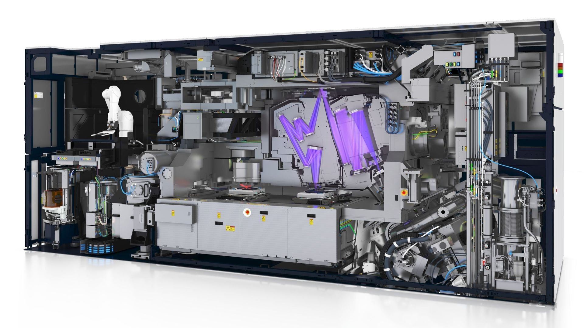
But moving to the extreme ultraviolet wavelength of 13.5 nm represented a true paradigm shift, extending to all aspects of light generation, reflective optics, vacuum environment management, wafer stage alignment and a host of other fields.
Only through its long-term and close collaboration with chipmakers, research partners and strategic suppliers such as ZEISS and TRUMPF, ASML learned to harness EUV light for industrial-scale chip manufacturing. The result was the NXE:3400B, which started shipping in 2017. Now used in the most advanced nodes of several major chipmakers, the system facilitated the introduction of multiple products with EUV-enabled chips to the consumer market in 2019.
“Outstanding engineering and industry achievements should be recognized and honored when they prompt new and emerging technologies to enhance the semiconductor industry,” said SEMI Americas president Dave Anderson. “Limitations of UV and immersion UV lithography presented a barrier for chipmakers and halted temporarily the downsizing of microelectronics. ASML’s years-long efforts drew supply chain support as well as customer buy-in, demonstrating that the industry can tackle major problems when it joins together.”
Martin van den Brink agreed, highlighting ASML’s commitment to not only working together but the advancement of technology. “It has been a long journey of highs and lows,” he said. “But a constant factor has been the creativity and dedication of our employees around the world. Over the coming 10 years, we will continue to see substantial innovations in the EUV’s productivity, imaging and overlay performance. The future of Moore’s Law is brighter than ever.”


