5-minute read - ASML, February 16, 2022
Moore's Law has been the guiding principle of progress in the semiconductor industry for over 55 years. As recent developments and industry roadmaps show, Moore's Law is set to continue even as the developments driving it are changing.
In 1965, Gordon Moore – the then director of R&D at Fairchild Semiconductor who would later go on to found chip manufacturer Intel – wrote a magazine editorial on the future of semiconductor chips in the coming ten years. That article included a simple observation on the technological capabilities and economics of chip production to that date.
"The complexity for minimum component costs has increased at a rate of roughly a factor of two per year. Certainly over the short term this rate can be expected to continue, if not to increase. Over the longer term, the rate of increase is a bit more uncertain, although there is no reason to believe it will not remain nearly constant for at least 10 years. That means by 1975, the number of components per integrated circuit for minimum cost will be 65,000."
Cramming more components onto integrated circuits, Electronics, Volume 38, Number 8, April 19, 1965
The prediction part of this statement was no more than a continuation of the then current rate of progress. Moore himself later described it as "a wild extrapolation". However, that extrapolation held true and people in the industry began to extend it further forward in time.
Over time, this observation came to be seen as the guiding principle of progress in the semiconductor industry: Moore's Law. But in truth, it was never an actual 'law' in the scientific sense. While it did describe the industry's impressive achievements historically, its predictive power was more as a (highly ambitious) target or roadmap that the semiconductor industry imposed on itself. Its adoption as such was driven more by the economics – the desire to keep microchip functionality moving forward at an affordable price – than any physical principle.
An ever-evolving constant
While we talk about Moore's Law surviving for over 50 years, it has regularly evolved over that time. Moore's original observation about complexity at minimum component cost has been translated into various equivalent statements, and the Law is now most often expressed as a rate at which the number of transistors on a chip doubles.

That rate of doubling has also changed according to progress in the industry and technology (something Moore himself predicted in 1975): from the original one year up to two years, which remains the pace of the industry. But while the fine details have changed, the essence of Moore's Law as a roadmap for development at a breathtaking pace has remained.
That shrinking feeling
Originally, this progress and doubling of transistor counts was delivered through three factors described by Moore as increased die size, dimension reduction (more commonly known as dimensional scaling or shrink), and device and circuit cleverness.
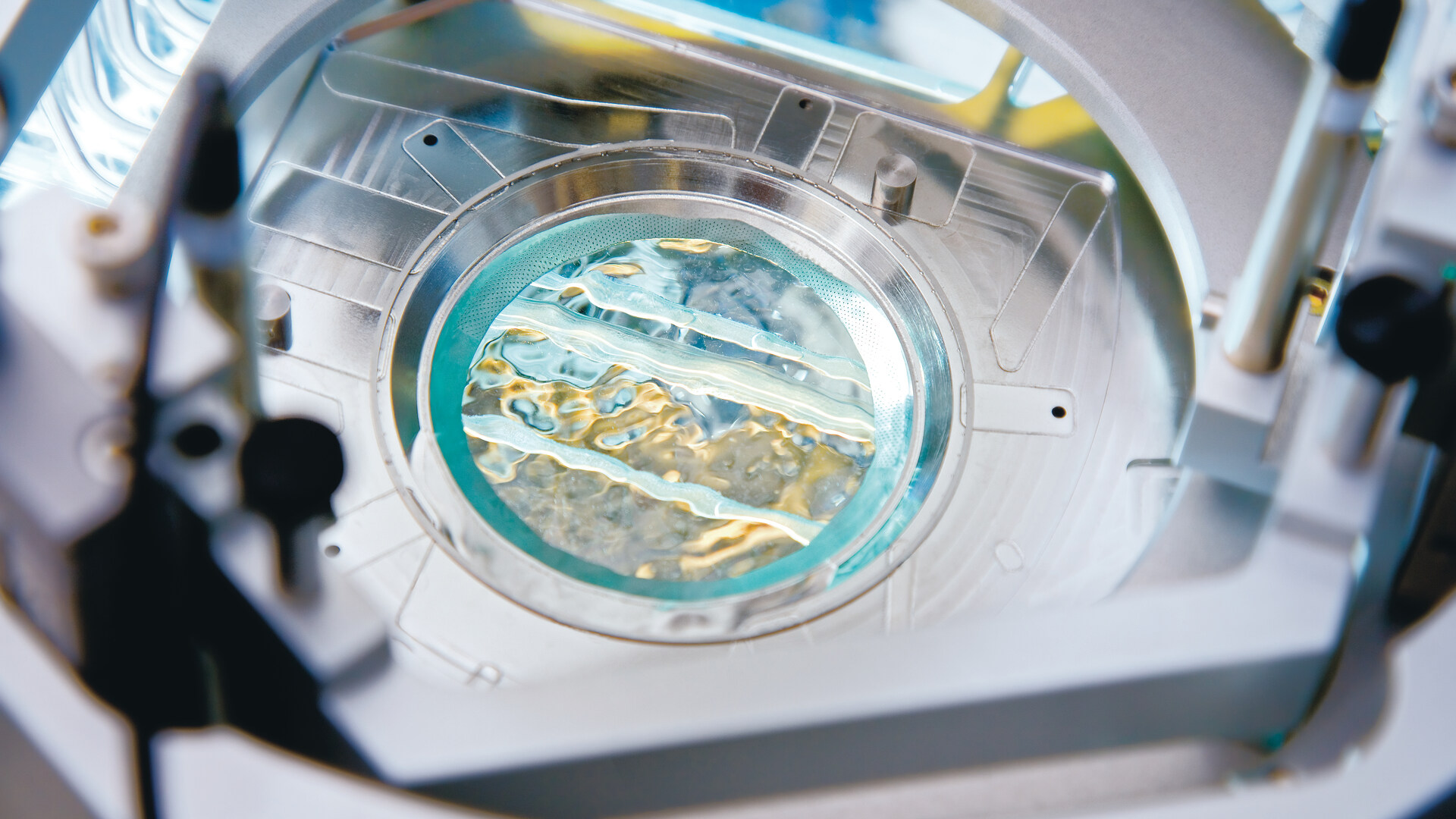
Dimensional scaling is largely driven by developments in lithography processes and technologies. Over the decades, this has included a migration to shorter wavelengths of ultraviolet light and an increased opening angle of the lens – the numerical aperture (NA) – as well as the introduction of immersion lithography, multiple patterning strategies and, most recently, EUV lithography.
As lithography enabled smaller features to be printed, chipmakers could pack more transistors into the same area, allowing the functionality of chips to increase while keeping costs affordable. As a result, dimensional scaling allowed the semiconductor industry to keep pace with Moore's Law for more than four decades.
The end of the road?
Smaller transistors operate faster and require less power. As a result, Moore's Law has become synonymous with the ongoing drive to improve chip performance and energy efficiency. However, at a certain point, the small size starts to interfere with the transistor's operation, breaking the relationship between size and performance, and energy efficiency.
For the type of transistors used in most microchips to date, the industry was nearing this breaking point around the mid-2000s. Transistors were still getting smaller at the same pace, but the resulting improvements in chip performance were slower.

New ways forward
However, as Moore reflected in 1975, making smaller features is only one way to improve chip performance. For decades, the semiconductor industry has also boosted chip performance through device and circuit cleverness – innovations in the materials and structures used to make transistors. This approach is known as device scaling. For example, the use of materials such as 'low-k dielectrics' improves the electrical properties of transistors.
More radically, new transistor architectures are continually being developed to overcome the size limitations of traditional transistor. To this end, the industry has launched chips based on so-called FinFETs which use thin but relatively high structures on the silicon surface that resemble fins. FinFETs are among the first of a new type of transistor known as 3D transistors.
Dimensional and device scaling involve evolution in the transistors themselves. In recent years, performance gains have also been achieved by innovation at the system level, allowing further scaling using existing transistor technologies.
One way to achieve this is through greater on-chip integration such as with system-on-chip solutions which combine processors, memory and auxiliary functionality into one chip, and 3D NAND flash, where multiple layers of flash memory are manufactured on top of each other to increase storage capacity from the same area. Another option is to integrate multiple optimized chips into a complete system using novel packaging solutions, often by stacking chips on top of each other.
The next ten years
Together, these approaches have kept Moore's Law in good health for the last 15 years. And looking at roadmaps across the industry, there is good evidence that they will maintain it through the next decade and beyond.
Certainly on the device side, there is enough planned innovation to continue the scaling roadmap to at least the 1 nm node with gate-all-around FETs, nanosheet FETs, forksheet FETs and complementary FETs among the more promising possibilities. These developments will be complemented by further dimensional scaling driven by improvements in lithography resolution (expected to shrink by a factor of two every six years or so) and accuracy as measured by the edge placement error (EPE).
ASML's continuous drive for innovation will support this trend. Our EPE roadmap, which is key to our holistic lithography portfolio, will be enabled by further improvements to lithography platforms and developments within our applications (including metrology and inspection) roadmap. EUV lithography, a technology unique to ASML, is now in high-volume production allowing simpler, cost-effective production at the 5 nm node. We're also currently working on our next generation lithography platform – High-NA (EUV 0.55 NA) – which will allow single-exposure production at around the 1 nm node.

In addition, we can expect system-level scaling to play a much greater role than it has to date. In the last year, memory makers produced 3D NAND chips with 176 memory layers on top of each other and announced roadmaps towards chips with more than 600 memory layers by around 2030. Beyond that, what shape the innovation will take is less known. However, if the 55-year history of Moore's Law has shown us anything, it is that the semiconductor industry is full of ideas for new developments. And as long as we still have ideas, Moore's Law will remain alive and kicking.
Want to dive deeper?