5-minute read - by Sander Hofman, October 3, 2022
The race for the microchip industry’s fastest, finest and most energy-efficient circuitry is intensifying among the world’s largest manufacturers. That’s why chipmakers are integrating brand-new transistor designs in their most advanced chip nodes. One of the most talked-about transistor designs is the gate-all-around transistor, which TSMC, Samsung and Intel have all announced they will be using in the coming years.
What is a transistor?
A transistor is a semiconductor component that amplifies or switches electrical signals. It’s one of the building blocks of modern electronics, including chips. Most of today’s chips contain billions of transistors.
How do transistors work?
Transistors make up the basic fabric of a chip. All transistors are interconnected and act as switches for electrical current. These gates turn on and off, either allowing or preventing current from passing through. This means that each transistor can be in two different states, storing two numbers – zero and one. With billions of transistors, a chip can contain billions of zeros and ones, sending, receiving and processing a remarkable amount of digital data. Just like any switch, a transistor needs to do three things exceptionally well: allow the maximum amount of current to flow through when it’s on, allow little to no current to leak when it’s off, and switch on and off as quickly as possible to guarantee optimal performance.
What are gate-all-around transistors?
Gate-all-around or GAA transistors are an upgraded transistor structure where the gate can come into contact with the channel on all sides, which makes continuous scaling possible.
What makes gate-all-around transistors superior?
To understand what makes GAA transistors better, we must first look at how transistor design has evolved over time, from planar to FinFET to GAA.
-
Planar transistors
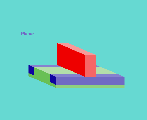
The classical transistor is called a planar transistor because it brings key elements of a transistor on a two-dimensional plane, including the gate, which modulates conductivity through a channel, the source, through which drive current enters the channel, and the drain, where current leaves the channel. All these components are built on a base of the semiconducting material silicon. This transistor concept was industrialized in the 1950s and 60s and was highly suited for mass production and miniaturization. The number of transistors a chip could contain increased significantly, giving rise to Moore’s Law and the chip industry as a whole.

-
FinFET transistors
Over time, engineers discovered that it’s possible to exert more control over the flow of current in the channel by raising the channel above the plane of the silicon, like a fin above water. Soon, the industry made the switch from 2D planar transistors to 3D fin field-effect transistors, abbreviated as FinFETs. In FinFET transistors, the gate wraps around the channel on three sides of a silicon fin, as opposed to across its top as in planar transistors. This creates an inversion layer with a much larger surface area, which allows the gate to better control the flow of current through the transistor. This means that more current can flow through with less leakage, and a lower gate voltage is needed to operate the transistor. In addition, the vertical geometry of FinFETs made it possible for engineers to pack more transistors in a chip, advancing Moore’s Law even further. The result was a chip with better performance, lower power consumption and a leading status through the 2010s.

-
Gate-all-around transistors
However, it was only a matter of time before FinFET technology would fall short of industry expectations. With the state-of-the-art chip nodes that TSMC, Samsung and Intel are manufacturing, FinFETs are reaching the limit of how high fins can go and how many fins can be placed side by side to boost their current-carrying capacity without suffering from electrical challenges.
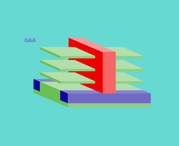
To further improve the control of the transistor channel, engineers found a way to replace the vertical fin with a stack of horizontal sheets, creating a new concept called gate-all-around field-effect transistors, which are shortened to GAA transistors, or GAAFETs. Gate-all-around transistors use stacked nanosheets. These separate horizontal sheets are vertically stacked so that the gate surrounds the channel on all four sides, further reducing leakage and increasing drive current. This means superior electrical signals pass through and between the transistors, improving chip performance. Additionally, chipmakers now have the flexibility to vary the width of the nanosheets to best suit a particular chip design. Specifically, wide nanosheets allow for higher and better drive current, while narrow nanosheets can optimize power consumption.

How will gate-all-around transistors change our daily life?
GAA transistors are poised to become part of the most advanced chip designs in the coming years. Because these transistors can be manufactured at a desirable cost for chipmakers, they will help keep the mass production of advanced chips affordable, while driving up the performance of new electronics, 5G connectivity, gaming, graphics, AI solutions, medical technology, automotive technology and more. Additionally, GAA transistors have better performance, less leakage and lower energy consumption, making them a more sustainable, environmentally friendly alternative to older designs.
Want to join us as an engineer at ASML? Check out our latest R&D jobs.


