ArF light source
Resolution
Projection optics
Wafers per hour
Key features & benefits
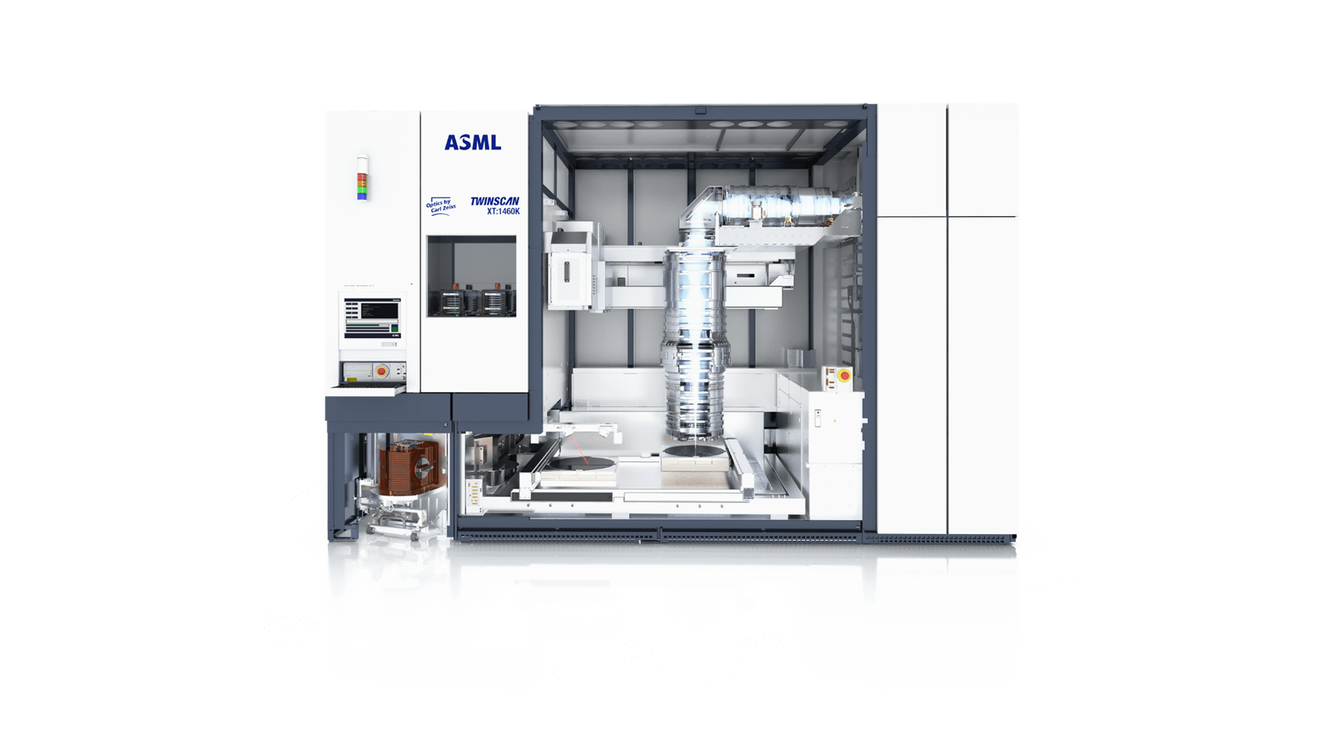
The TWINSCAN NXT:1470 193 nm step-and-scan system is the first ever “dry” lithography system built on our high-productivity, high-precision NXT platform. As a result, it is the first dry system to achieve on-product overlay better than 4.5 nm – and the first lithography machine of any kind capable of processing more than 300 wafers per hour.
With its outstanding overlay and throughput performance, this dual-stage ArF lithography tool helps chip manufacturers reduce cost per exposure while producing up to 50% more wafers from the same lithocell footprint. It will enable the planned KrF NXT systems to further reduce the cost of chip production while improving matched-machine overlay for higher yields.
01. Productivity
With its NXT body – featuring a new generation of wafer stage module – the NXT:1470 delivers up to 50% greater throughput than our previous fastest ArF system. It is supported by an ongoing roadmap to increase productivity even further, helping manufacturers continue to improve the cost effectiveness of high-volume chip production.
02. Optics
The TWINSCAN NXT:1470 features a variable-NA (0.70 – 0.93) Carl Zeiss Starlith 4X reduction lens. Compared to our previous dry ArF lithography systems, it includes an additional lens element and enhanced improvements for lens heating control.
03. Imaging performance
The TWINSCAN NXT:1470 is built on the latest version of our NXT high-throughput, high-precision system architecture, featuring improved wafer stages and wafer handlers. Combined with the enhanced optics and improved lens and reticle heating control, it enables on-product overlay below 4.5 nm – while processing over 300 wafers per hour.
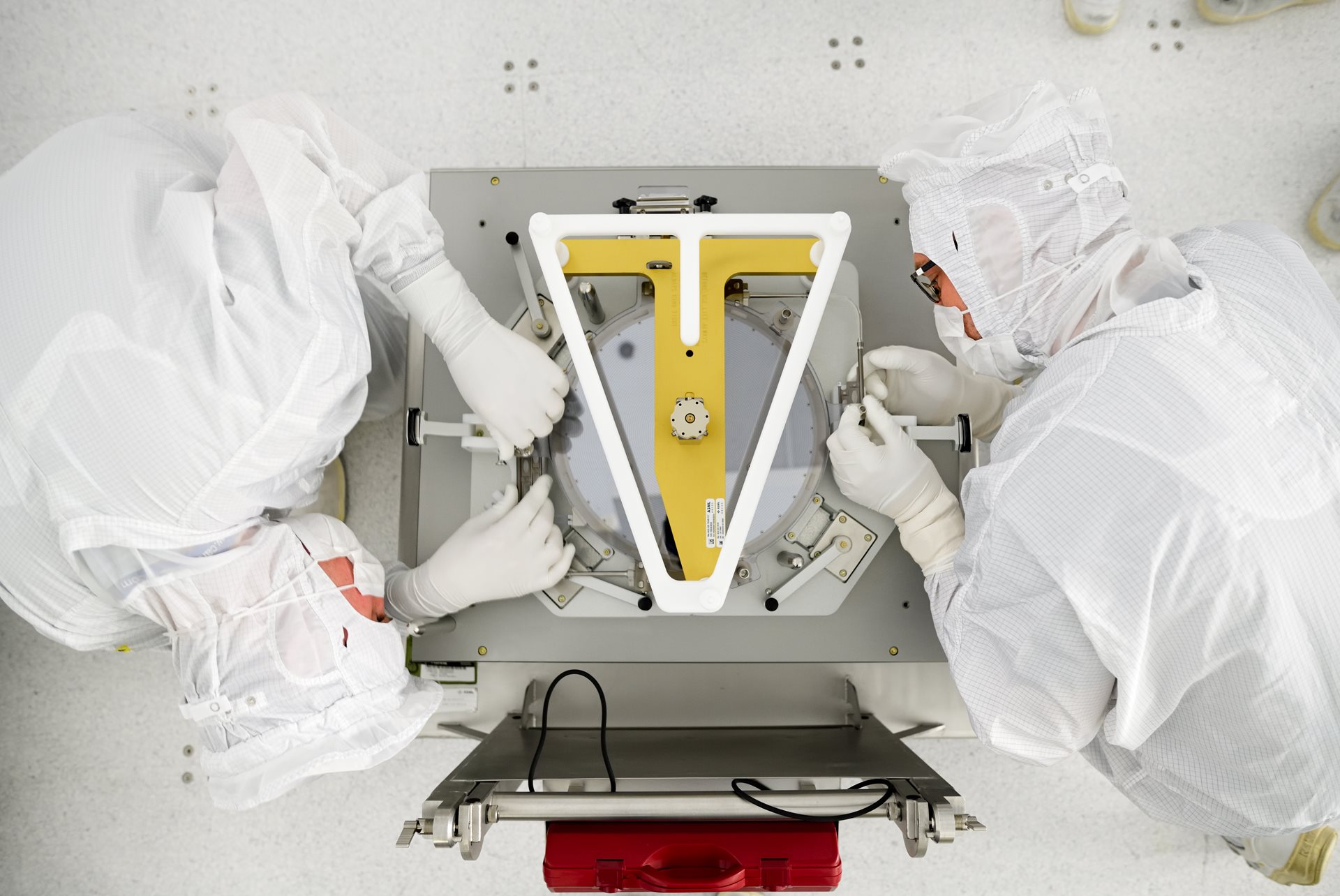
With polarized illumination, the NXT:1470 can reach production resolutions down to 57 nm. In addition, latest UV level sensor ensures superior focus control over the full wafer, especially for edge dies.